3D Circuit Integration Technology for Multiproject Fabrication
150 likes | 516 Vues
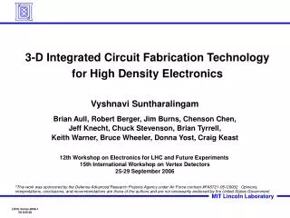
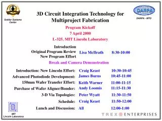
3D Circuit Integration Technology for Multiproject Fabrication. 7 April, 2000 James Burns, Andy Curtis, Paul Davis, Andy Loomis, Jim Reinold, Keith Warner, Peter Wyatt, Craig L. Keast, keast@LL.mit.edu MIT Lincoln Laboratory Lexington MA, 02173. Outline. Background

3D Circuit Integration Technology for Multiproject Fabrication
E N D
Presentation Transcript
3D Circuit Integration Technologyfor Multiproject Fabrication 7 April, 2000 James Burns, Andy Curtis, Paul Davis, Andy Loomis, Jim Reinold, Keith Warner, Peter Wyatt, Craig L. Keast, keast@LL.mit.edu MIT Lincoln Laboratory Lexington MA, 02173
Outline • Background • Motivation for 3-D technology • Why Multiproject Fabrication? • Leveraging the FDSOI CMOS technology base • Current Status • Photodiode process development • 3-D technology transfer • Wafer Aligner/Bonder purchase • 3-D Via topologies • Summary
3-D Circuit Technology • General Objective • Break away from the traditional 2-D-constrained Moore’s Law scaling trends by developing and demonstrating a robust, high density, vertical chip-to-chip interconnection technology and making it available to the DoD and research community through multiproject runs • Program Description (Joint effort with TREX Enterprises) • Develop enabling technologies for 3-D integration • Precision wafer-to-wafer overlay • Low temperature wafer-to-wafer oxide bonding • High density wafer-to-wafer electrical interconnects • Demonstrate the 3-D technology by fabricating a high definition 3-layer imaging module • Put in place infrastructure to allow for 3-D multiproject fabrication
Motivation: 3-D Circuit Technology Mixed Material System Integration High Bandwidth m-Processors Exploiting Different Process Technologies Advanced Imaging Technologies Large Focal Planes • Better circuit / interconnect ratio • “Unrestricted” vertical interconnections between layers • Low digital system power: P=CV2f SOI CMOS 3D
Via Isolation SOI Buried Oxide Plan View 10-mm thick epi layer Handle Wafer SOI Buried Oxide Metal 1 Pad Via Isolation Handle Wafer 6 mm 3-D Interconnect Demonstration Vehicle(Fully Parallel 64 x 64 APS Imager with A/D Conversion) A/D Converter Circuits fabricated in 1-mm thick SOI CMOS Active Pixel Imaging Circuits fabricated in 10-mm thick SOI CMOS
Deep Via Cross Sectional SEM Deep Via Back Metal A/D Metal-1 Adhesive Imager Metal-1 Imager Metal-2 Imager Silicon 5 mm 3-D Process FlowBack Metal Interconnect
Developing 3-D Multiproject Infrastructure • Transfer to, enhance and stabilize all aspects of the 3-D fabrication process in Lincoln’s Microelectronics Laboratory • Initial program effort had different parts of the 3-D fabrication process being performed at three different locations • Starting circuit layer fabrication: MIT Lincoln Laboratory • Wafer transfer and bonding: Kopin Corporation • 3-D via etch and metallization: Northeastern University • Demonstrate 3-D circuit technology by fabricating a three-layer high definition imaging module SOI CMOS signal processing (layer 3) SOI CMOS A/D Converter (layer 2) Imaging Layer (layer 1) Thinned Bulk Si Wafer Backside illumination
Motivation:3-D Multiproject Fabrication • Mainstream silicon technology continues to focus on 2-D centered technologies • This approach will probably continue for another ~10+ years unless something “revolutionary” happens • This is the low risk path, lots of inertia in the system • Maximizing the potential of 3-D system architecture requires a new “thought process” • We need to get a group of talented individuals and/or teams thinking about the design/architecture issue as it relates to specialized DoD and potential commercial system needs • This thinking needs to be focused in the context of a realizable 3-D technology
Motivation:3-D Multiproject Fabrication(cont.) • The 3-D Multiproject Fabrication model provides the vehicle to explore the potential of 3-D system integration across a broad research interest base • Putting in place a “user friendly” streamlined 3-D integration technology built upon • Aggressive low power, high performance SOI CMOS technology • Robust oxide-based wafer bonding technology • Precision wafer-to-wafer alignment technology • Provides the opportunity to explore mixed function (MEMS, CMOS, CCD, etc.) and mixed material (Si, SiGe, GaAs, etc.) system integration • Builds upon Lincoln Laboratory’s past Multiproject Run experience and core process technologies already in place and under development at the Laboratory
Low Power, High Performance FDSOI CMOS Roadmap FY98 FY99 FY00 FY01 FY02 0.10 mm SOI CMOS MUMS3 Ship 6/14/99 MUMS2 Ship 7/15/98 Baseline 0.25 mm SOI/CMOS MUMS4 Start 1/1/00 0.175 mm SOI/CMOS Merged CCD/CMOS DoD/AS&T MUMS3.5 Start 2/1/99 LVA1 Start 4/1/00 LVA2 Start 11/1/00 DoD/R&T Low Voltage Analog DARPA/ARMY 3-D Stacking Technology Honeywell/LM Damascene Waveguides 3-D Layer Stacking RF MEMS Precision-MCM-D FDSOI CMOS InGaAs Detectors Rad Hard 0.175 mm SOI/CMOS DoD/DTRA Integrated 3-D Microsystems
Advanced Photodiode Development Photodiode Process Simulation • Current CMOS processes support diode fabrication but: • Leakage currents are too high for low noise photodiodes • Substrate doping too high for large depletion regions and high quantum efficiency • We are developing an enhanced photodiode process for the 3-D effort based on existing Lincoln Laboratory photodiode technology Microns Microns
3-D Technology Transfer • Original program had process activities at: MIT-LL, NEU, and Kopin • All of these process activities are now being integrated in the the MIT-LL Microelectronics Laboratory tool set • Wafer-to-wafer alignment and void-free bonding • 3-D via etching • 3-D via interconnect metallization 150-mm Diameter Wafer Pair (Bonded and Thinned)
Wafer Aligner/Bonder Purchase Wafer-to-Wafer Alignment (Bottom side referenced) • 3-D Integration Program requires a precision wafer-to-wafer overlay and bonding system • We have researched the currently available commercial tools • Barely satisfactory for the current 3-D mutiproject demonstration effort • Clearly unsatisfactory for commercial 3-D fabrication • Technology exists to make the necessary system but there is currently no market demanding the capabilities of such a tool
M1 M1 W3 Shallow vias M3 W2 Deep vias W1 M4 M4 M1 M1 M2 M3 Glue M3 M2 M1 M1 Si wafer 3-D Via Topologies • Currently designing a mask set which will serve as the “workhorse” for developing the robust 3-D interconnect technology • Supports 2 and 3-layer stacking • Allows for the investigation of both topside-up and flipped wafer stacking techniques • Investigates multiple layer-to-layer via interconnect topologies • Designed for automated electrical characterization
Summary • Developing the technology base necessary for demonstrating a robust 3-D circuit interconnect technology • Original demonstration program was a team effort with Northeastern University and Kopin Corporation • 64 x 64 imager with A/D conversion (>4,000 3-D interconnects) Sample Image • Follow-on multiproject effort is a collaboration between Lincoln Laboratory and a commercial technology transfer partner (TREX Enterprises) • Transferring, while enhancing and streamlining, the 3-D technology into the MIT Lincoln Laboratory “commercial” tool set • Program demonstrator is a three-layer, high definition (1280 x 1024) imaging module • Goal is to make 3-D multiproject prototyping available in 2002