Download
1 / 74
770 likes | 1.33k Vues
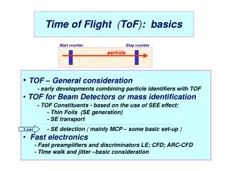
Time of Flight ( ToF ) : basics. Start counter. Stop counter. TOF – General consideration - early developments combining particle identifiers with TOF TOF for Beam Detectors or mass identification - TOF Constituents - based on the use of SEE effect:

E N D
Time of Flight (ToF): basics Start counter Stop counter • TOF – General consideration • - early developments combining particle identifiers with TOF • TOF for Beam Detectors or mass identification • - TOF Constituents - based on the use of SEE effect: • - Thin Foils (SE generation) • - SE transport • ------------------------------------------------------------------------------------------------------------------------------------------------------------- • - SE detection ( mainly MCP – some basic set-up ) • Fast electronics • - Fast preamplifiers and discriminators LE; CFD; ARC-CFD • - Time walk and jitter –basic consideration 2. part
Timing measurements • Pulse height measurements discussed up to now • emphasize accurate measurement of signal charge • Timing measurements optimize determination of time of • occurrence timing output signal ( “time stamp”) • For timing, the figure of merit is notthe Signal / Noise ratio • but the Slope / Noise ratio
Fast Timing • Timing measurements Detectors for • Timing and their FEE • - Scintillator & Photomultiplier assembly • - MCPs & Fast Preamplifiers • - Semiconductor detectors & Preamplifiers • ( CSP vs. Current ) • b) Ultra-fast Timing Circuits and Signal • - Time - stamp • - Time - walk and Time - jitter
3rd layer 1st layer 2nd layer ~300 ps ~250 ps ~350 ps 244Cm 241Am239Pu Time of Flight [ns] ( ~200 keV energy loss ) Counts IKP - TOF & BPM Preliminary results - 250 +/- 50 ps - coincidence with energy measurements (SC + DGF-4C-rev.F) - transparent beam detector and tracking with 32x SC matrix as Stop detector (real beam test is requested!) Counts 239Pu 241Am 244Cm 5.155 5.486 5.804 [MeV]
a) Timing measurements Detectors for • Timing and their FEE • - Scintillator & Photomultiplier assembly • - MCPs & MCP-PMT and Fast Preamplifiers • and very briefly about other ultra-fast detectors • - Semiconductor detectors (Si, Diamond) & their Preamplifiers • ( CSP vs. Current )
Scintillators & Photomultiplier tubes (PMT) Detector Photomultiplier tube - (PMT) Gain ~ 106 sec.secondary electrons / photo-electron Different geometries of PMT Circular-cage type PMT
Box-and-grid type PMT and the typical electron trajectories Linear-focused type PMT
The transparent window material commonly used in PMT: - MgF2 crystal ; - Sapphire ; - Synthetic silica; - UV glass; - Borosilicate glass Transmittance (%) Wavelength (nm) Basic Photocathode commonly used in PMT: - Cs-I 100 M - Cs-Te 200 S;M - Bialkali (Sb-Rb-Cs, Sb-K-Cs) 400 U;S;K - Multialkali (Sb-Na-K-Cs 500 K;U;S - Ag-O-Cs 700K;S-1 - GaAsP(Cs) Photocathode Radiant sensitivity (mA/W) Wavelength (nm)
Photons • transport • WLS WLS Wavelength shifter Detector
Signal output problem and the solution Countermeasures for very fast response circuits (the “miraculous” (small) series resistor and not parallel capacitor) The effect of damping resistor on ringing ( remember the influence of resistor in the quality factor of an oscillator or larger capacitor value in a low-pass frequency filter :) C - filter-change the frequency ! Rs –oscillation damper !
The importance of Poles and Zeros Pole-zero diagram Ideal oscillator real oscillator - R series e.g. 10 pF * 10 nH 500 MHz Step 2 Step 1 Step 3
Going from PMT ( Photomultiplier Tube) • to MCP (Microchannel Plate) • from a discrete dynode structure to a • continuous distributed dynode structure but also • more than 8 orders of magnitude scaled down • design in volume • ( 102 in length and > 103in diameter )
Multi-channel Plate Detectors Electroding (on both face) Channels - e initial velocity ( ~1eV) - channel length/diameter ratio Kc- constant
Metallized ++ Metallized+ • Much stable operation vs. external high magnetic fields in comparison with PMT • lower gain but in chevron configuration the gain ~106 • lower power consumption (gain vs. HV) MCP assembly in chevron configuration
MCPs in Single, vs. Chevron and Z-stack configurations Gain: 103-104 106 108
MCP gain dependence vs. - parameter and stage configuration MCP gain dependence vs. channel diameter and technology Comparison of gain characteristics of three different types of 2-stage MCPs Comparison of gain characteristics of various single and multi stage MCPs
Comparison of timing characteristics of chevron 2-stage MCP-PMT, one with 6 µm and another with 12 µm pore diameter
Mesh form anode ( e.g. X,Y delay lines signal pulse amplitude only 15-20% compared to the solid anode standard version) ? • Hamamatsu • R-3809 U-50 • Photocathode • diam. ~10mm • Price - ! HV ~ 3 kV Rise time ~150ps Fall time ~350 ps FWHM ~ 300 ps Standard operating circuit for an MCP-PMT
Anode Return Path Problem Current out of MCP is inherently fast- but return path depends on where in the tube the signal is, and it can be long and so rise-time is variable Incoming Particle Trajectory Signal Would like to have return path be short, and located right next to signal currentcrossing MCP-OUT to Anode Gap The Signal is a current and not a potential 10cm wire; 0.2mm diam 150 nH Impedance @ 1Ghz ~ 1 kOhm 10 pF ~ impedance @ 1GHz ~ 1.5 kOhm Signal & Return Load
Detector Signal Collection High Z Circuit development Low Z • Impedance adaptation • Amplitude resolution • Time resolution • Noise cut Voltage source + Zo Z Rp - Low Z T Quo vadis ? • Low Z output voltage source circuit can drive any load • Output signal shape adapted to subsequent stage (ADC) • Signal shaping is used to reduce noise (unwanted fluctuations) vs. signal
+ Rp Z - Detector Front-end electronics – overview Detector as fast signal generator electron-hole pairs collection only electrons (or particles) if Z is high charge is kept on capacitor nodes and voltage builds up (until capacitor is discharged) • Advantages: - excellent E resolution - friendly pulse shape analysis • Disadvantages: - channel-to-channel crosstalk - pile up above 40 k c.p.s. - sensitivity to e.m.c. ~ Ci FEE (Input stage)
+ Rp Z ~ Ri - Detector Front-end electronics – overview Detector as fast signal generator electron-hole pairs collection only electrons (or particles) if Z is low charge flows as a current through the impedance in a short time. • Advantages: - limited signal pile up - limited channel-to-channel crosstalk - low sensitivity to parasitic signals - good timing resolution • Disadvantages: - pour signal/noise ratio - sensitive on return GND loop ! FEE (Input stage)
Capacitive Return Path Solution Return Current from anode Current from MCP-OUT
~25mm Ultra-fast detectors, extremely user-friendly solutions, the only disadvantages: - small area of photocathode and extremely expensive
Chemical Vapour Deposition techniques CERN - LHC experiment CVD-Diamond
the CVD - Diamond Detectors Two “optical grade” CVD and ~ 100µm thickness • a 30 x 30 mm2 detector with 9 strips • with a pitch of 3.1 mm and • a 20 x 20 mm2 pixel detector with a • pixel size of 4.5 x 4.5mm2 • the first large-area CVD diamond detectors • Installed at SIS The largest diamond detector of 60 x 40 mm2 and ~200µm thickness <0> in the focal plane detector of a magnetic spectrometer E. Berdermann et al, CVD-Diamond Detectors… Nucl. Phys. B 78 (1999), 533 E. Berdermann et al, The use of CVD-Diamond for heavy ions… Diamond and Related Materials 10(2010),1770
Charge Sensitive Preamplifier • Active Integrator (“Charge Sensitive Pre-Amplifier”) • Input impedance very high ( i.e. NO signal current flows into amplifier) • Cf(Rf ) feedback capacitor (resistor) between output and input • very large equivalent dynamic capacitance • sensitivity A(∆qi) ~ q / Cf • large open loop gain Ao ~ 10,000 - 150,000 • very fast active integrator • tr < 1ns (sub-nanosecond CSP) • A0 ~ 1,000-10,000 • Transconductance amplifier • ASIC integrated structure ∆Qi Ci E. Berdermann et al, The use of CVD-Diamond for heavy ions… Diamond and Related Materials 10(2010),1770
Standard current amplifier solution G2 G1 G1 > G2 to minimize S/N ratio HSMP 3862 series tr ~ 1.2 ns (10 to 90%) Imax (1µs)~ 1A Peak Inverse Voltage ~50V Tj –Max. Junction Temperature ~ 150°C (OK to be used in vacuum) Simulation results of the amplifiers with THS 3201 ultra-fast current feedback amplifier
Signal Output A1. A2. A3 . e Noise Output A1.A2.A3. e1 + A2.A3. e2 + A3.e3 the gain of the first block of amplification must be kept as high as possible, in order to reduce the importance of the noise contributions coming from the following blocks i.e. the preamplifier gain has to be as large as possible ! Ao >>10 4
Ultra-fast Timing Circuits and Signal • -Time-stamp • - Time-walk & Time-jitter as perturbation effects • * Timing – time stamp but actually timing means measurement oftime intervals(from fs to ms) • Walk effect - variation of time stamp (timing) caused • by signal variation in amplitude and/or rise time • Jitter effect - timing fluctuations caused by noise and/or • statistical fluctuations in the detector (intrinsic noise) • two identical signal will not always trigger at the • same point (time stamp) time variation dependent • on the amplitude of fluctuation – slope/noise ratio
“MVP “ in fast time domain tra ~ tc The noise bandwidth approaches the signal bandwidth the timing jitter
- the Ortec 579 – to slow for fast timing New fast amplifiers: - Ortec 9327 (1 GHz Amplifier and Timing Discriminator) - Ortec 9309-4 ( Quad Ultra-Fast Amplifier) - Ortec 9306 (1-GHz Preamplifier)
this is the reason while only • 1-2 amplifier stages * • * this can be implemented only • if the product [gain x bandwidth] • of the amplifier is large enough ! 10 cm wire; 0.2 mm diam 150 nH Impedance @ 1Ghz ~ 1 kOhm 1 pF ~ impedance @ 1GHz ~ 150 Ohm Simulation results of the amplifiers with THS 3201 ultra-fast current feedback amplifier
Gain ~7 (th. 10) Gain ~10 (th. 20) Current Feedback Amplifier THS-3201 Main features: - 1.8 GHz; - 6700 V/µs @ G= 2V/V; RL=100 Ohm - 18mA @ +/- 3.3V (120mW vacuum) tr ~ 1.2 ns (10 to 90%) Simulation results of the amplifiers with THS 3201 ultra-fast current feedback amplifier
Wire impedance skin effect (i.e. skin depth calculator) R0 = 1 /πro2 σ (DC & low frequencies) - σ bulk conductivity -r0 wire radius L0= μ / 8π - μpermeability (μ0 = 4π.10-7 Henry/Meter) Rs = 1/(σδ); q = √2 r0/ δ δis the “skin depth” (πfμσ)-1/2 • * to remember about skin effect: • Material dependence • (e.g. Ni vs. Cu ~ skin effect • depth one order of magnitude) • - Frequency dependence * - this “calculator” only cover the range q < 8 Which roughly correspond to r0/δ < 5 … above this value the Bessel functions become hard to evaluate…
Time walk Time walk for a fixed trigger level time stamp (time of threshold crossing) depends on pulse amplitude • Accuracy of timing • measurement is limited • by two factors: • time jitter( ~ to the slope/noise) • time walk *) • (due to dependency on signal • amplitude and rise time variations) • *) - if the rise time is known and constant, • the “time walk” can be compensated in • software event-by-event by measuring the • pulse height and correcting the timing • - if rise time vary (e.g. HP-Ge Det.) this • technique fails! PSA required Hardware: - threshold lowest practical level (i.e. > noise) or compensation technique (e.g. CFD)
LE – method • timing occurrence function of: • - amplitude • - rise time • - noise Time Walk in LE discriminator due to: - amplitude and rise time variations - charge sensitivity Time jitter in LE discriminator due to: - noise on the Input Signal - pulse high variation
Constant Fraction Timing + -- Ideal comparator • Implementing an “active threshold”, namely • the threshold is derived from the signal passing • it through an attenuator Vt = f Vs ; (f < 1) • The signal applied to the comparator input the • transition occurs after the threshold signal reached • Its maximum value: VT = f V0 tr
The circuit compensates for amplitudes and rise time if pulses have a sufficiently large range that extrapolates to the same origin delayed input signal attenuated input signal Timing occurrence at the output