Download
1 / 17
180 likes | 395 Vues
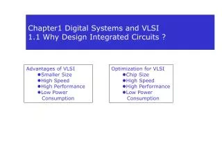
Chapter1 Digital Systems and VLSI 1.1 Why Design Integrated Circuits ?. Advantages of VLSI Smaller Size High Speed High Performance Low Power Consumption. Optimization for VLSI Chip Size High Speed High Performance Low Power Consumption.

E N D
Chapter1 Digital Systems and VLSI1.1 Why Design Integrated Circuits ? Advantages of VLSI • Smaller Size • High Speed • High Performance • Low Power Consumption Optimization for VLSI • Chip Size • High Speed • High Performance • Low Power Consumption
1.2 Integrated Circuit Manufacturing1.2.1 Technology • A series of identical chips are patterned onto the Wafer. • Some space is reserved for test circuit structures. Wafer
Physical Design = Layout • Stick diagram to represent
1.2.2 EconomicsMoore’s Law • The transistor counts would double every 18 months. • Standard LSI communication network I/O graphics accelerators floating point processors • ASICS(Application Specific IC) • Memories
1.3.2 Power Consumption • Power Consumption limits the number of transistors on a chip. • Low Power Design --- Low heat in battery-operated systems like cellular telephones and personal digital assistants (PDA). • Low Power Design Architecture Level Logic Level Circuits Level Layout Level
1.3.3 Design and Testability • Design Test to check design fault • Manufacturing Test to check manufacturing defects • Common Fault Model: stuck-at-0/1 (the defect causes a logic gate’s output to be always 0 ( or 1), and occurs one at a time) • Testability Scan Path methods, Self test circuits
1.4.1 Hierarchical Design • Multiple levels of abstraction System, Architecture, Logic, Circuit, Layout • Multiple and Conflicting Costs cost/area, function, speed, power consumption • Short Design Time
Pins on a component • Component=body+pins • Definition of Type (entity) = full_adder instances=> full_adder1 full_adder2 ----- full_adderN • N-bit Adder=N full_adderI
A hierarchical logic design net2 • Net List (component List) net1: top.in1 i1.in net2: i1.out xxx.B top.in1: top.n1 xxx.xin1 top.in2: top.n2 xxx.xin2 top.in3: top.n3 xxx.xin3 net3: xxx.out i2.in outnet: i2.out top.out
Dynamics of Dynamic Latch 0 1 1 0 Data Store Data Hold
Digital Logic AbstractionConcept of Rise & Fall Time • Rise & Fall time depends on equivalent RC time constants. R = On resistance of MOS transistors. C = Parasitic Capacitance at Output Ports
Concept of Delay • The values of nodes are fixed to 0 or 1. Delay of gates produces Delay of digital systems.
Large register-transfer systems • Figure shows Data Path of 3 input additions. Adders: combinational logic Or logic with registers
A typical design abstraction ladder for digital systems Top-down design Bottom-up design