Download
1 / 36
450 likes | 846 Vues
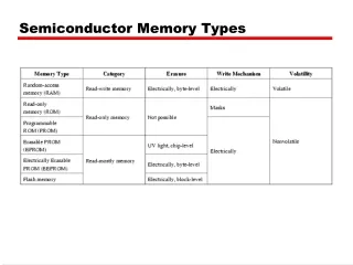
Semiconductor Memory. Issues in Flash Memory NOR vs. NAND Multilevel cell: 2-bit cell Threshold voltage distribution Reliability Endurance, Retention, Program disturb Scaling Limitation due to oxide thickness Limitation due to amount of charge High level Data Management

E N D
Semiconductor Memory • Issues in Flash Memory • NOR vs. NAND • Multilevel cell: 2-bit cell • Threshold voltage distribution • Reliability • Endurance, Retention, Program disturb • Scaling • Limitation due to oxide thickness • Limitation due to amount of charge • High level Data Management • Page allocation scheme and Block cleaning • Interfacing • Latency
Semiconductor Memory Non-Volatile Memory Comparison Source : Rabaey
Semiconductor Memory Random Access Memory (volatile) • STATIC (SRAM) • Data stored as long as supply is applied • Large (6 transistors/cell) • Fast • Differential signaling • DYNAMIC (DRAM) • Periodic refresh required • Small (1-3 transistors/cell) • Slower • Single ended signaling
Semiconductor Memory • SRAM • 64Kb SRAM array
Semiconductor Memory • SRAM : differential signaling • Symmetrical data path to obtain reliable operation at full speed
Semiconductor Memory WL V DD M M 5 6 Q M Q M 4 3 M M 1 2 BL BL 6-transistor CMOS SRAM Cell VDD M5 M6 Q Q M1 M2 GND M3 M4 WL BL BL Source : Rabaey
Semiconductor Memory • SRAM Read • Prechargebothbitlines high • Then turn on wordline • One of the two bitlines will be pulled down by the cell • Ex: q = 0, qb = 1, bit discharges, bit_b stays high while q and qb bump slightly • Read stability Conditions • q must not flip • M1 >> M3 (typically 3-4 times)
Semiconductor Memory • SRAM Write • Drive one bitlinehigh, the other low • Then turn on wordline • Bitlines overpower cell with new value • Ex: q = 0, qb = 1, bit = 1, bit_b = 0 • Force qb low, then q rises high • Writability Conditions • Must overpower feedback inverter • M4 >> M6 (typically 1.5 times)
Semiconductor Memory Resistance-load SRAM Cell WL V DD R R L L Q Q M M 3 4 BL BL M M 1 2
Semiconductor Memory Resistance-load SRAM Cell • Replace PMOS with resistors • Undopedpolysilicon can make TΩ/sq • Reduce static power dissipation • Need only IR > 10-13 A to compensate leakage current • Reduce wiring and contacts • Reduce size by one-third PMOS Thin-Film Transistor SRAM Cell • Increase cell reliability • Less sensitivity to leakage and soft error • Lower standby current than resistive load
Semiconductor Memory DRAM • Invented by IBM researcher (1T) but first marketed by Intel (3T) • Store binary data as charge on capacitance • In contrast to the SRAM, no constraints exist on the device size ratio • In 1T cell read process is destructive thus stored data must be regenerated every time they are read • Due to charge leakage, stored data need periodically refresh • Many variations in the realization, depending on the number of polysilicon layers, method of capacitor formation, conductors used for row and column
Semiconductor Memory 1T DRAM Source : Rabaey
Semiconductor Memory DRAM Write 1/0 • Data value is placed on BL (1/0) • When the WL rises, the capacitor CS is either charged (write 1) or discharged (write 0) Source : Rabaey
Semiconductor Memory DRAM Read 1 • Capacitor CS stored 1, Vx = VBIT ,BL is first precharged to Vdd/2 = VPRE • WL rises, CS shares its charge with CBL • BL voltage increases to VBL Source : Rabaey
Semiconductor Memory V V (1) BL V ∆ PRE V (1) V (0) t Sense amp activated Word line activated Typical bit line voltage during the readout Source : Rabaey
Semiconductor Memory DRAM Read 1 • ∆V change in BL will be amplify to Vdd by sense amplifier • CBL≈ 10 CS typical CS≈ 30fF, ∆V ≈ 200 mV • During the readout output of sense amp is imposed onto the bit line to restore the charge • Read and Refresh are intrinsically intertwined
Semiconductor Memory DRAMwith Trench Capacitor • Capacitance value ~20 – 30 fF Source : Harris
Semiconductor Memory DRAM with Stack Capacitor • Two additional Poly-Si are deposited above the transistor with a dielectric material sandwiched between them • Capacitance value ~ 20 - 30 fF in 0.35µm • CBL ~200 - 300fF Source : Hodges
Semiconductor Memory Periphery • Decoders • Sense Amplifiers • Input/Output Buffers • Control / Timing Circuitry Source : Rabaey
Semiconductor Memory Hierarchical Decoders • Multi-stage implementation improves performance Structure of two-level decoder for 6-bit address Source : Hodges
Semiconductor Memory V DD V DD V DD V DD Dynamic Decoders Precharge devices GND GND WL 3 WL 3 WL 2 WL 2 WL 1 WL 1 WL 0 WL 0 V A A A A f DD 0 0 1 1 A A A A f 0 0 1 1 2-input NAND decoder 2-input NOR decoder Source : Rabaey
Semiconductor Memory BL BL BL BL 0 1 2 3 S 0 A 0 S 1 S 2 A S 1 3 D Column Decoder BL BL BL BL 0 1 2 3 A 0 A 0 2-input NOR decoder A 1 A 1 D pass-transistor based tree based Source : Rabaey
Semiconductor Memory Differential Sense Amplifier V DD M M 3 4 y Out M M bit bit 1 2 M SE 5 Directly applicable toSRAMs Source : Rabaey
Semiconductor Memory Differential Sensing -SRAM V V DD DD PC BL BL V V DD DD EQ M M y y 3 4 WL i M M 1 2 x x x x SE SE M 5 SE SRAM cell i V DD Diff. x x Output Sense y Amp SE Output (a) SRAM sensing scheme (b) two stage differential amplifier Source : Rabaey
Semiconductor Memory Latch-Based Sense Amplifier -DRAM EQ BL BL V • Initialized in its meta-stable point with EQ DD SE • Once adequate voltage gap created, sense amp enabled with SE • Positive feedback quickly forces output to a stable operating point. SE Source : Rabaey
Semiconductor Memory Issues in volatile memory • SRAM and DRAM are operate under low signal-to-noise conditions • Supply voltage reduction • Capacitance reduction • Increased integration density raises the noise level due to inter-signal coupling (capacitive crosstalk) • Wordline-to-bitline coupling • Bitline-to-bitline coupling • High-speed requirement increases switching noises • Soft error more pronouncing
Semiconductor Memory Noise Sources in 1T DRAM substrate BL Adjacent BL C WBL -particles WL leakage C S electrode C cross
Semiconductor Memory WL-BL Coupling (DRAM) • Review capacitive crosstalk • Coupling capacitance CWBL between WL and BL causes charge-redistribution
Semiconductor Memory Solution: open bit linearchitecture • Memory array is divided in to two halves, differential amp placed in the middle. On each side dummy cells is added. EQ L L L V R R L 1 0 DD 0 1 SE BLL BLR … … C C C C C C S S S SE S S S Dummy cell Dummy cell Source : Rabaey
Semiconductor Memory Leakage • Sub-threshold current to BL more serious due to low Vth • Tunneling leakage current more serious due to thin oxide • pn junction leakage is small since cell is small • Leakage current across field oxide. Trench isolation can help BL BL+1 WL Itunnel Ijunc Isub Icell-to-cell
Semiconductor Memory Data Retention Dissipation SRAM • Increasing Vth using body biasing • Inserting extra resistance in the leakage path • Lowering supply voltage DRAM • Dynamically controlled Vth: well biasing access transitor • Turn off device hard : apply a negative voltage on WL • Raise bit line voltage of unused cells
Semiconductor Memory Density Improvement • Deep sub-micron feature size • Stacked capacitor in DRAM • High dielectric constant material such as BST • SOI-DRAM results in better isolation (Z-RAM) Various Access Methods • Fast page mode (FP) • Extended data output (EDO) • Synchronous DRAM (SDRAM) • Double data rate (DDR) • Direct Rambus DRAM (DRDRAM)
Semiconductor Memory Row Address Redundant rows Fuse : Bank Redundant columns Memory Array Column Column Decoder Address Redundancy in memory array increases the yield. Source : Jan Rabaey
Semiconductor Memory SRAM vs. DRAM Source : S. Natarajan, et al, IEEE Solid-State Circuits Magazine v1 no3 2009
Semiconductor Memory • Embedded SRAM vs. DRAM – Scaling Trend • Embedded DRAM is three to five times denser in the same technology Source : S. Natarajan, et al, IEEE Solid-State Circuits Magazine v1 no3 2009
Semiconductor Memory • Embedded SRAM vs. DRAM • Standby current increases as device gets smaller Source : S. Natarajan, et al, IEEE Solid-State Circuits Magazine v1 no3 2009