Download
1 / 7
70 likes | 73 Vues
In the field of cryptography, optical information processing low power CMOS design and nanotechnology Reversible logic has found its applications and has become one of the promising research directions This paper presents a novel and quantum cost efficient combinational circuits for nanotechnology. This gate can work singly as a reversible full adder unit and requires only one clock cycle. The proposed gate is a universal gate in the sense that it can be used to synthesize any arbitrary Boolean functions. It has been demonstrated that the hardware complexity offered by the proposed gate is less than the existing counterparts. The proposed reversible circuits are then compared with different reversible circuits Ankita Jain | Ashish Raghuwanshi "A Design and Implementation of Reversible Logic Based Combinational Circuit with low Quantum Cost" Published in International Journal of Trend in Scientific Research and Development (ijtsrd), ISSN: 2456-6470, Volume-1 | Issue-6 , October 2017, URL: https://www.ijtsrd.com/papers/ijtsrd2477.pdf Paper URL: http://www.ijtsrd.com/engineering/electronics-and-communication-engineering/2477/a-design-and-implementation-of-reversible-logic-based-combinational-circuit-with-low-quantum-cost/ankita-jain<br>

E N D
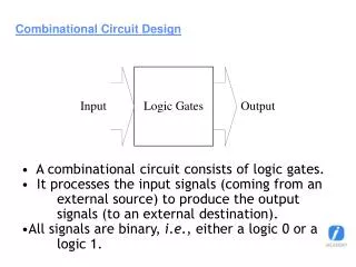
International Research Research and Development (IJTSRD) International Open Access Journal A Design and Implementation of Reversible Logic Based Combinational Circuit with Low Quantum Cost International Journal of Trend in Scientific Scientific (IJTSRD) International Open Access Journal ISSN No: 2456 ISSN No: 2456 - 6470 | www.ijtsrd.com | Volume 6470 | www.ijtsrd.com | Volume - 1 | Issue – 6 A Design and Implementation of Reversible Logic Based Combinational Circuit with A Design and Implementation of Reversible Logic Based ow Quantum Cost Ankita Jain Department of Electronics & IES College of Technology, Bhopal, India Ashish Raghuwanshi Ashish Raghuwanshi Department of Electronics & Communication Engineering, IES College of Technology, Bhopal, India M. Tech. Student, Department of Electronics & Communication Engineering, IES College Technology, Bhopal, India Assistant Professor, Department of Electron Communication Engineering, Technology, Bhopal, India ABSTRACT In the field of cryptography, optical information processing low power nanotechnology Reversible logic has found its applications and has become one of the promising research directions this paper presents a novel and quantum cost efficient combinational circuits for nanotechnology. This gate can work singly as a reversible full adder unit and requires only one clock cycle. The proposed gate is a universal gate in the sense that it can be used to synthesize any arbitrary Boolean functions. It has been demonstrated that the hardware complexity offered by the proposed gate is less than the existing counterparts. The proposed reversible circuits are then compared with different reversible circuits input vectors can be uniquely recovered from its corresponding output vectors. Bennett [2] showed that zero energy dissipation is possible only if the gating network consists of reversibility will become future trends towards low power dissipating circuit design. power dissipating circuit design. input vectors can be uniquely recovered from its corresponding output vectors. Bennett [2] showed that zero energy dissipation is possible only if the gating network consists of reversibility will become future trends towards low In the field of cryptography, optical information processing low power nanotechnology Reversible logic has found its applications and has become one of the promising CMOS CMOS design design and and reversible reversible gates. gates. T Thus sents a novel and quantum cost efficient combinational circuits for nanotechnology. This gate can work singly as a reversible full adder unit and requires only one clock cycle. The proposed gate is a universal gate in the Reversible logic design differs significantly from traditional combinational logic design approaches. In reversible logic circuit the number of input lines must be equal the number of output lines, each output will be used only once and the resulting circuit must be acyclic [3]. The output lines that are not used further are termed as garbage outputs. One of the most challenging tasks is to reduce these challenging tasks is to reduce these Reversible logic design differs significantly from traditional combinational logic design approaches. In reversible logic circuit the number of input lines must ual the number of output lines, each output will be used only once and the resulting circuit must be acyclic [3]. The output lines that are not used further are termed as garbage outputs. One of the most esize any arbitrary Boolean functions. It has been demonstrated that the hardware complexity offered by the proposed gate is less than the existing counterparts. The proposed reversible circuits are then compared with different garbages [3]. Any reversible logic gate realizes only the functions that are reversible. But many of the Boolean functions are not reversible. Before realizing these functions, we need to transform those irreversible functions into reversible one. Any transformation algorithm that converts an irreversible function to a reversible one introduces input lines that are set to zero in the circuit’s input side [4 inputs are termed as constant inputs. Therefore, any efficient 0.......reversible logic design should mini the garbages as well as constant inputs. the garbages as well as constant inputs. ny reversible logic gate realizes only the functions that are reversible. But many of the Boolean functions are not reversible. Before realizing these functions, we need to transform those irreversible functions into reversible one. Any rithm that converts an irreversible function to a reversible one introduces input lines that are set to zero in the circuit’s input side [4-5]. These inputs are termed as constant inputs. Therefore, any efficient 0.......reversible logic design should minimize Keywords: reversible logic, reversible logic Component, Component, floating floating point point adder, adder, 1.INTRODUCTION Power dissipation is one of the most important factors in VLSI circuit design. Irreversible logic circuits dissipates kT*log 2 Joule (k is the Boltzmann constant and T is the absolute temperature) heat for every and T is the absolute temperature) heat for every ower dissipation is one of the most important factors in VLSI circuit design. Irreversible logic circuits dissipates kT*log 2 Joule (k is the Boltzmann constant bit of information that is lost irrespective of their implementation technologies [1]. Information is lost when the input vectors cannot be recovered from circuit’s output vectors. Reversible logic naturall takes care of heating since in reversible circuits the takes care of heating since in reversible circuits the bit of information that is lost irrespective of their implementation technologies [1]. Information is lost when the input vectors cannot be recovered from circuit’s output vectors. Reversible logic naturally This paper presents a novel 4*4 reversible gate namely Peres Full Adder Gate (PFAG) , that is, it has 4-input lines and 4-output lines. This gate can be used to realize any arbitrary Boolean function to realize any arbitrary Boolean function and therefore This paper presents a novel 4*4 reversible gate namely Peres Full Adder Gate (PFAG) , that is, it has output lines. This gate can be used @ IJTSRD | Available Online @ www.ijtsrd.com @ IJTSRD | Available Online @ www.ijtsrd.com | Volume – 1 | Issue – 6 | Sep-Oct 2017 Oct 2017 Page: 62
International Journal of Trend in Scientific Research and Development (IJTSRD) ISSN: 2456-6470 universal. The hardware complexity of this gate is less compared to the existing ones and requires only one clock cycle. The quantum realization cost of this gate is only 8 and ready for use in depends on any particular realization of quantum logic. Generally, the cost is calculated as a total sum of 2*2 quantum primitives used. The cost of Toffoli gate is exactly the same as the cost of Fredkin gate and is 5. The only cheapest quantum realization of a complete (universal) 3*3 reversible gate is Peres gate and its cost is 4. Table 1.1 Truth table of Irreversible X-OR Gate A 0 0 1 1 B 0 1 0 1 P 0 1 1 0 Figure 2.1: 2*2 Feynman Gate Figure 1.1: Irreversible EX-OR Gate Table 1.2 Truth table of Reversible X-OR Gate A B P Q 0 1 0 0 0 1 0 0 Figure 2.2: 3*3 Fredkin Gate 0 1 1 1 1 0 1 1 Here P represents the Garbage output Figure 1.2: Reversible EX-OR Gate Figure 2.3: 3*3 Tofolli Gate II. REVERSIBLE LOGIC GATES There exist many reversible gates in the literature. Among them 2*2 Feynman gate [6] (shown in figure2), 3*3 Fredkin gate [7] (shown in figure 2.2), 3*3 Toffoli gate [8] (shown in figure 2.3) and 3*3 Peres gate [9] (shown in figure 2.4) is the most referred. The detailed cost of a reversible gate @ IJTSRD | Available Online @ www.ijtsrd.com | Volume – 1 | Issue – 6 | Sep-Oct 2017 Page: 63
International Journal of Trend in Scientific Research and Development (IJTSRD) ISSN: 2456 International Journal of Trend in Scientific Research and Development (IJTSRD) ISSN: 2456 International Journal of Trend in Scientific Research and Development (IJTSRD) ISSN: 2456-6470 Figure 3.1 Peres Full Adder Figure 3.1 Peres Full Adder This PFA (Peres Full Adder) can be taken as a block in order to facilitate the notation of its expansion. The inputs order was also changed to better fit in an This PFA (Peres Full Adder) can be taken as a block in order to facilitate the notation of its expansion. The inputs order was also changed to better fit in an expansion diagram. Figure 2.4: 3*3 Peres Gate 3*3 Peres Gate III Combinational Circuit III Reversible Reversible Logic Logic Implementation Implementation of of A.Design of 1 bit Full Adder Full adder is the fundamental building block in many computational units. The anticipated paradigm shift logic compatible with optical and quantum requires compatible reversible adder implementations. The full adder circuit’s output is given by the following equations: Full adder is the fundamental building block in many computational units. The anticipated paradigm shift logic compatible with optical and quantum requires compatible reversible adder implementations. The full adder circuit’s output is given by the following Figure 3.2 PFA as a block PFA as a block Once we take the FPA as a block, we can derive the algorithm to implement an n-bits adder. This algorithm was implemented in this design and can be Once we take the FPA as a block, we can derive the algorithm to implement an n algorithm was implemented in this design and can be seen in figure 3.3 Sum = A B Cin Cout = (A B) Cin AB AB The reversible logic implementation of full circuit and other adder circuits and their minimization issues has been discussed in . It has been shown in [11] and [13] that any reversible logic realization of full adder circuit includes at least two garbage outp and one constant input. The author in [10 given a quantum cost efficient reversible full adder circuit that is realized using two 3*3 Peres gates only (shown in figure 3.1). This implementation of reversible full adder circuit is also efficient gate count, garbage outputs and constant input than the existing counter parts. ible logic implementation of full-adder circuit and other adder circuits and their minimization issues has been discussed in . It has been shown in [11] and [13] that any reversible logic realization of full adder circuit includes at least two garbage outputs and one constant input. The author in [10-13] has given a quantum cost efficient reversible full adder circuit that is realized using two 3*3 Peres gates only (shown in figure 3.1). This implementation of reversible full adder circuit is also efficient in terms of gate count, garbage outputs and constant input than For this implementation, I will be using the Peres gate as it is the gate with the lower quantum cost as can be seen in the figures 3.1. The Peres’ implemented Ful Adder with its corresponding quantum cost can be seen below: For this implementation, I will be using the Peres gate as it is the gate with the lower quantum cost as can be seen in the figures 3.1. The Peres’ implemented Full Adder with its corresponding quantum cost can be Figure 3.3: 4-bits adder implementation bits adder implementation @ IJTSRD | Available Online @ www.ijtsrd.com @ IJTSRD | Available Online @ www.ijtsrd.com | Volume – 1 | Issue – 6 | Sep-Oct 2017 Oct 2017 Page: 64
International Journal of Trend in Scientific Research and Development (IJTSRD) ISSN: 2456-6470 fredkin gate. The quantum cost of modified fredkin gate is 4[12]. For given inputs corresponding outputs are resulted as x0 ,x1,x2,x3,x4,x5,x6,x7. B. Design of 2x4 reversible decoder with low quantum cost and minimum garbage output. Figure below shows the circuit of 2x 4 decoder using one feyman gate and two modified fredkin gate. The quantum cost of modified fredkin gate is 4[12]. For given inputs corresponding outputs are resulted as x,y,w,z. Figure 3.5: Reversible 3X8 decoder Figure .3.4: 2x4 reversible decoder IV. Result and Simulation C. Design of 3x8 reversible decoder The venture was reenacted with the assistance of the Xilinx ISE 9.2 instrument. Table 3.1 Truth table of 3x8 reversible decoder Table above shows the truth table for 3x8 reversible decoder and figure below shows the circuit of 3x 8 decoder using one feyman gate and six modified Figure 4.1 Graph showing comparison in existing and proposed quantum cost and garbage output @ IJTSRD | Available Online @ www.ijtsrd.com | Volume – 1 | Issue – 6 | Sep-Oct 2017 Page: 65
International Journal of Trend in Scientific Research and Development (IJTSRD) ISSN: 2456-6470 The combinational circuit full adder is designed using peres gate and 2x4 decoder , 3x8 decoder is designed using modified feyman gate and modified fredkin gate are analyzed in terms of quantum cost and garbage output. different combination our simulation of full adder is correct. Table 4.1 Comparison between quantum cost and garbage output Figure 4.3 Simulation result of 1 bit full adder The figure below shows the RTL architecture of 3x8 decoder with minimum quantum cost and garbage output The figure below shows the RTL view of 1 bit full adder with low quantum cost and minimum garbage output Figure 4.4 RTL Schematic of 3x8 reversible decoder Figure 4.2 RTL Schematic of 1 bit full adder Figure below shows the simulation result of 3x8 decoder with low quantum cost and minimum garbage output [1].From simulation result of 3x8 decoder we can check the desired output of decoder by assigning different combination of inputs and it can be checked with the truth table of decoder if our outputs are same Figure below shows the simulation result of 1 bit full adder with low quantum cost and minimum garbage output [1].From simulation result of 1 bit full adder we can check the desired output of full adder by assigning different combination of inputs and it can be checked with the truth table of full adder if our outputs are same as the output of the truth table for @ IJTSRD | Available Online @ www.ijtsrd.com | Volume – 1 | Issue – 6 | Sep-Oct 2017 Page: 66
International Journal of Trend in Scientific Research and Development (IJTSRD) ISSN: 2456-6470 as the output of the truth table for different combination our designed circuit is correct. Simulation result of 2:4 decoder Figure below shows the simulation result of 2x4 decoder with low quantum cost and minimum garbage output [1].From simulation result of 2x4 decoder we can check the desired output of decoder by assigning different combination of inputs and it can be checked with the truth table of decoder if our outputs are same as the output of the truth table for different combination our designed circuit is correct. Figure 4.5: Simulation of 3 x 8 reversible decoder 2X4 Reversible decoder Figure 4.7: Simulation result of 2x4 decoder The figure below shows the RTL architecture of 2X4 decoder with minimum quantum cost and garbage output [ 1] CONCLUSION In this dissertation combinational circuit like full adder, 2x4decoder, 3x8decoder are designed using reversible gate. These circuits are designed for minimum quantum cost and minimum garbage output. The method proposed can be generalized. The method of designing combinational circuit helps to implement many digital circuits with better performance for minimum quantum cost and garbage output. Future work related to building of proposed reversible logic by using technologies such as CMOS technology, in particular adiabatic CMOS, optical, thermodynamics, technology, nanotechnology and DNA technology is another important aspect. REFERENCES Figure 4.6 RTL View of 2x4 decoder [1] Gopi chand Naguboina et al: “Design and synthesis of combinational reversible decoder in Xilinx. IEEE Xplore 2017 intenational conference. circuit using @ IJTSRD | Available Online @ www.ijtsrd.com | Volume – 1 | Issue – 6 | Sep-Oct 2017 Page: 67
International Journal of Trend in Scientific Research and Development (IJTSRD) ISSN: 2456-6470 [2] H M H Babu, M R Islam, S M A Chowdhury: Synthesis of full-adder circuit using reversible logic. 17th International Conference on VLSI Design. Proceedings. IEEE Xplore: 24 August 2004 [11] Anindita Banerjee et al. “New design of reversible sequential devices” 12 august 2009 [12] Ankush et al “Design and performance analysis of low power reversible carry skip adder”IOSR Journal of VLSI and signal processing. [3]Junchaw Wing, Ken Choi: A Carry look ahead adder designed by reversible logic. SoC Design Conference (ISOCC), IEEE Xplore: 20 April 2015 2014 International [13] Anupam Chattopadhyay, Anubha Bhakshi “ Low quantum cost constructions for adder and symmetric Boolean function" 2016 International symposium on circuits and system, IEEE xplore 11 aug 2016. [4] Marcin Kerntopf , Marek Pawłowski , Andrzej Skorupski: Encryption using reconfigurable reversible logic gate and its simulation in FPGAs; Mixed Design of Integrated Circuits and Systems, 2016 MIXDES - 23rd International Conference IEEE Xplore: 04 August 2016 [5]R. Keyes and R. Landauer : "Irreversibility and Heat Generation in Process", IBM Journal Development, vol. 5, pp. 183-191, 1961 [6] W David Pan, Mahesh Nalasani; Reversible logic; IEEE Potentials ( Volume: 24, Issue:Feb.-March 2005 ) Bryk , Krzysztof Gracki , Paweł the of Computational Research and [7] H.Thapliyal and N. Ranganathan. Reversible logic based concurrent error detection methodology for emerging nanocircuits. In Nanotechnology (IEEE- NANO) 10th IEEE Conference on, pages 217 – 222, aug. 2010. [8]Design of a Reversible Floating-Point Adder Architecture by Michael Nachtigal and all in 2011 11th IEEE International Nanotechnology Portland Marriott Conference on . [9]Design of a Reversible Floating-Point Adder Architecture by Michael Nachtigal and all in 2011 11th IEEE International Nanotechnology Portland Marriott. Conference on [10] C H Bennet “Logical reversibility of computation” IBM Journal and dev, pp525-532 nov 1973 @ IJTSRD | Available Online @ www.ijtsrd.com | Volume – 1 | Issue – 6 | Sep-Oct 2017 Page: 68