Download
1 / 11
150 likes | 283 Vues
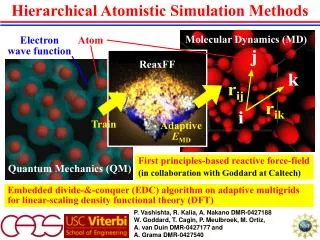
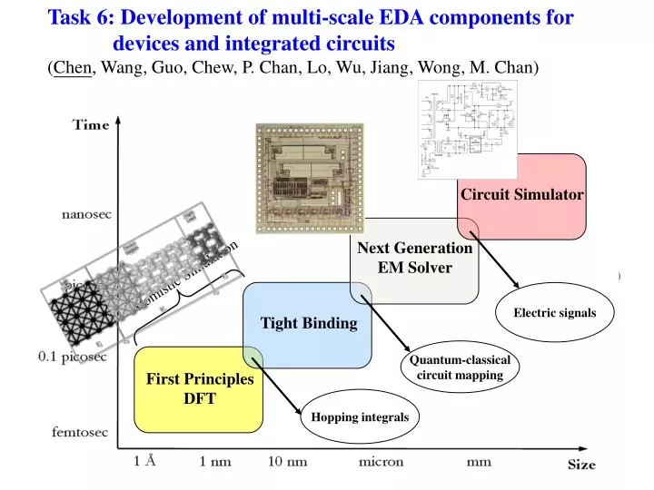
Task 6: Development of multi-scale EDA components for devices and integrated circuits ( Chen , Wang, Guo, Chew, P. Chan, Lo, Wu, Jiang, Wong, M. Chan). Next Generation EM Solver. Circuit Simulator. Tight Binding. First Principles DFT. Atomistic Simulation. Electric signals.

E N D
Task 6:Development of multi-scale EDA components for devices and integrated circuits (Chen, Wang, Guo, Chew, P. Chan, Lo, Wu, Jiang, Wong, M. Chan) Next Generation EM Solver Circuit Simulator Tight Binding First Principles DFT Atomistic Simulation Electric signals Quantum-classical circuit mapping Hopping integrals
DFT & TB for Quantum Transport (Guo, Wang) Non-equilibrium Green’s function (NEGF) method Landauer Formula: • Steady state • ω=0 & ω≠0 • 2. Time dependent
TDDFT for transient currents (Chen) boundary condition Left electrode right electrode system to solve ,mL ,mR Dissipation functional Q (energy and particle exchange with the electrodes) Poisson Equationwith boundary condition via potentials at SL and SR
Electromagnetics Solver (Chew, Jiang) Circuit Simulator (Wu, Jiang, P. Chan, M. Chan) PEEC, DPEC & etc.
Coupled EM-Semiconductor Simulation?N. Wong and Q. Chen Combine full-wave EM simulation and device simulation Advanced simulator must allow simultaneous simulation of on-silicon components (passives) and in-silicon components (actives) Device simulations EM simulations
Metal: Ohm’s law Semiconductor: Drift-Diffusion Basics: Maxwell Insulator Basic variables:
Interface Condition • Metal/insulator interface • Semiconductor/insulator interface • Metal/semiconductor/insulator interface Metal/semiconductor interface (ohmic contact)
Quantum Mechanics / Molecular Mechanics (QM/MM) Method QM MM
QM/EM Simulation • Replace devices of interests (drift-diffusion etc) by models using quantum mechanism (QM) • Since only a small portion of semiconductor can be handled by QM model, the interface between QM and classical model in solution scheme will be crucial QM EM
EM solver Atomistic details QM region QM region QM region PEEC/ DPEC
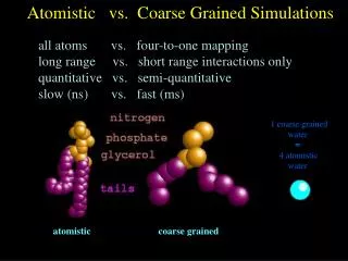
Multi-scale simulation methods (Engineering & Science) 1023 100~1000um Continuum scale Astronomy >>1,000,000 10um~100um Continuum model ~ 1,000,000 10~10um 1,000 ~100,000 atoms 1nm~10nm Finite element ~100 atoms 1Ǻ~1nm Atomic scale Coarse grain Molecular mechanics Quantum mechanics