Download
1 / 15
150 likes | 261 Vues
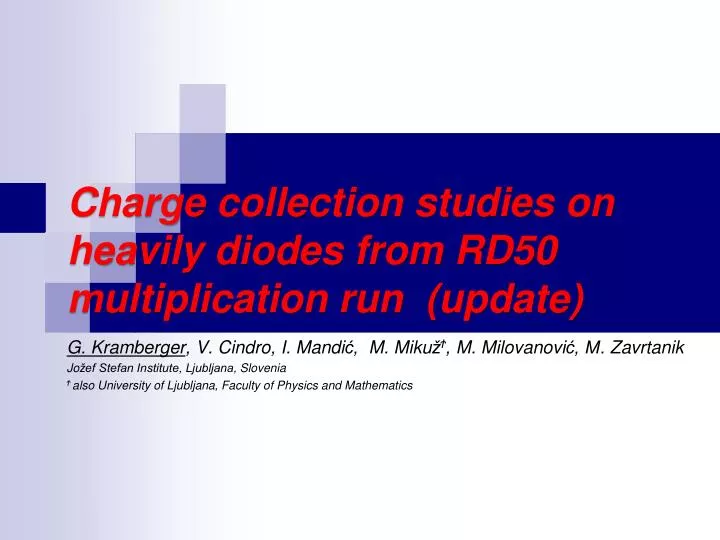
Charge collection studies on heavily diodes from RD50 multiplication run (update). G. Kramberge r , V. Cindro, I. Mandi ć, M. Mi ku ž Ϯ , M. Milovanovi ć, M . Zavrtanik Jo žef Stefan Institute, Ljubljana, Slovenia Ϯ also University of Ljubljana, Faculty of Physics and Mathematics.

E N D
Charge collection studies on heavily diodes from RD50 multiplication run (update) G. Kramberger, V. Cindro, I. Mandić, M. MikužϮ, M. Milovanović, M. Zavrtanik Jožef Stefan Institute, Ljubljana, Slovenia Ϯ also University of Ljubljana, Faculty of Physics and Mathematics
Motivation Additional information are in the talk at 20th RD50 Workshop: https://indico.cern.ch/getFile.py/access?contribId=15&sessionId=4&resId=1&materialId=slides&confId=175330 RD50 had/has a “multiplication wafer” run with Micron, which included special devices/diodes for studying impact of various parameters on charge collection: • Does implant diffusion time matter? • Does energy of implantation ions matter? • How much does thickness matter? In addition: • What is the wafer-to-wafer reproducibility? • How big is the is the difference between a pad diode and spaghetti diode? • Does long term annealing depend on material? • Are detector still alive at Feq~1017 cm-2? G. Kramberger, Charge collection studies on heavily diodes from RD50 multiplication run (update), 21th RD50 Workshop, 2012, CERN
Samples • Special diodes-pad detectors were designed on that wafers which are particularly suitable for studies of charge collection: • DC coupled, guard ring structure – high breakdown voltage • 80 mm pitch, 20 mm implant width (ATLAS geometry) • 4x4 mm2 , 300 and 150 mm thick • All strips connected together at one side: • almost the same electric field as in strip detector • much simpler handling (CCE, CV-IV etc. measurements) • weighting field has same shape as the electric field Type 3 (used in this work) Metalized implant G. Kramberger, Charge collection studies on heavily diodes from RD50 multiplication run (update), 21th RD50 Workshop, 2012, CERN
Tex2440 Amplifier +shaper pad detector 90Sr/241Am thermal isolation cold plate scintillator Peltier cooler water cooled heat sink Irradiations and measurements Type 3: samples from different wafers: 2935-2 – standard 2e15 cm-2, 150 keV P 2935-3- standard 5e15 cm-2, 80 keVB 2935-4– standard 220 nm thermal oxide 2935-5 - standard 2935-6 - standard 2935-7 – standard 2935-8 - standard 2935-9 – standard 2884-7 – standard 2935-10 - double diffusion (1000oC for 3h) 2912-2 - double energy 300 keV of P ions 2912-3 - double energy doubly charged ! 2885-5 – thin • Sample treatment: • Neutron irradiations: in steps up to 8∙1016 cm-2,80 min annealing at 60oC in between • Measurements done in the range [-20ºC, -25oC] • some samples irradiated to a fix fluence (single step) to check for consistency • some standard p-type diodes were also irradiated for comparison • Measurements: • CCE measurements with 90Sr setup • 25 ns shaping • 97% trigger purity • Calibrated for non-irradiated detector with 59.5 keV line from 241Am • I-V measured G. Kramberger, Charge collection studies on heavily diodes from RD50 multiplication run (update), 21th RD50 Workshop, 2012, CERN
CCE and noise for non-irradiated samples without detector ENC~2000 e variation of ~10% for charge at V>Vfd – several samples were re-measured and reproducibility was found to be better than that good agreement of Vfddetermined from Q-V with that of C-V Noise performance in accordance with expectations G. Kramberger, Charge collection studies on heavily diodes from RD50 multiplication run (update), 21th RD50 Workshop, 2012, CERN
CCE comparison for all wafers cm-2 cm-2 T=-23oC T=-23oC 80 min@60oC - 2 irr. steps 80 min@60oC • almost no difference in charge collection efficiency for different implants (but only limited parameter region of investigation) • superior performance of thin detectors (black squares) at lower voltages • very high CCE for thin detector (~10-11 ke for 3∙1015 cm-2). • up to 1000 V thin are at least as good as thick • only moderate increase of charge collection with high bias voltages for thin device – why don’t we see larger increase of multiplication? G. Kramberger, Charge collection studies on heavily diodes from RD50 multiplication run (update), 21th RD50 Workshop, 2012, CERN
CCE of “standard” wafers for all fluences 3e15 1e16 2e16 4e16 8e16 Even at 8∙1016 cm-2 a signal of ~1200 e can be expected i.e. few mip sensitivity with present electronics An interesting observation – at very high fluences (2,4,8∙1016 cm-2) no problems with micro discharges – very stable operation! G. Kramberger, Charge collection studies on heavily diodes from RD50 multiplication run (update), 21th RD50 Workshop, 2012, CERN
Dependence of CCE on voltage 500 V: a=2.69e14 , b=-0.675 800 V: a=3.40e14 , b=-0.695 1000 V: a=4.16e14 , b=-0.68 G. Kramberger, Charge collection studies on heavily diodes from RD50 multiplication run (update), 21th RD50 Workshop, 2012, CERN power law dependence of QMVP on fluence (“an empirical formula”) surprisingly works over two orders of magnitude! almost constant in collected charge for different voltages at given fluence
Leakage current performance scaled to -20oC for 1016 cm-2 volume generation current 1016 cm-2 3∙1015 cm-2 thin sample …, but the Ileak is a sum of guard and bulk currents Leakage current larger than given by volume bulk does not scale precisely with fluence (factor ~3) – difference in MI ? G. Kramberger, Charge collection studies on heavily diodes from RD50 multiplication run (update), 21th RD50 Workshop, 2012, CERN
Leakage current and noise at high fluences 2935-9 T=-23oC • Leakage current at given voltage doesn’t scale with fluence (even at voltages below “expected Vfd” ) and shows a tendency to saturate. Reasons: • reduced multiplication at very high fluence ? • saturation of responsible generation centers? • Low noise for higher irradiated devices in spite of large leakage current? • At lowest fluence the onset of micro discharges can be seen in the noise. G. Kramberger, Charge collection studies on heavily diodes from RD50 multiplication run (update), 21th RD50 Workshop, 2012, CERN
Annealing of wafers with different implants There is no systematic difference between different implants in terms of CCE during long term annealing Thin detector performs best also during long term annealing The slope of the charge rise with voltage increases with annealing – seen already several times before (CERN, JSI, Glasgow…) CCE>1 for the thin device already at 600 V after 5120 min @ 60oC G. Kramberger, Charge collection studies on heavily diodes from RD50 multiplication run (update), 21th RD50 Workshop, 2012, CERN
Annealing of wafers with different implants The Q-V plot shows rapid rise of charge after 1280 min annealing At low bias voltages the charge is smaller for longer annealing times (<400 V) Increase of noise is related to increase of charge, but a detector with smaller electrodes would have larger S/N (series noise should dominate over shot noise) I-V has a similar shape as Q-V with a difference because of generation current annealing (initial drop of current) Similar behavior seen for all investigated materials. G. Kramberger, Charge collection studies on heavily diodes from RD50 multiplication run (update), 21th RD50 Workshop, 2012, CERN
Difference between pads and strips weighting field for spaghetti diode (3 strips) 80min@60oC Two standard FZ-p pad detectors from Micron were used for comparison (2551-4 wafer) irradiated to the same fluence: • the difference between pad and spaghetti is large • can not the due to weighting field Qe/(Qe+Qh)=0.53 , diode~0.5 • can be due to multiplication, but the difference is there also at low voltages • Relative difference is somewhat larger at larger fluence (not conclusive) G. Kramberger, Charge collection studies on heavily diodes from RD50 multiplication run (update), 21th RD50 Workshop, 2012, CERN
Difference between pads and strips weighting field for strip detector (middle of the 5 strip segment) Two standard FZ-p strip detectors of the same strip geometry from Micron were used for comparison irradiated to the same fluence: • the difference between strip and spaghetti is relatively small, very likely due to multiplication (note larger fluences as for pads) • The difference comes from the weighting field and charges induced in the neighbors (see I. Mandic’s talk) spaghetti strip G. Kramberger, Charge collection studies on heavily diodes from RD50 multiplication run (update), 21th RD50 Workshop, 2012, CERN
Conclusions & future work • New “spaghetti” diodes perform well • Within the parameter space investigated in RD50 Micron Multiplication run: • the “double energy” of implantation ions and • the “double diffusion time” processed diodes perform equally after irradiation and also during long annealing to spaghetti diodes processed in a standard way • Thin diodes perform better than standard ones for both fluences for bias <=1000 V • Strong increase of charge during long term annealing, but also noise and leakage current • As expected the spaghetti diodes perform better than standard pad diodes (multiplication?) and worse than strip detectors (trapping induced charge sharing) at given fluence. • Spaghetti diodes are still “alive” at 8∙1016 cm-2– the charge of 1250 e can be expected (probably more for strip detectors) at 1000 V . Further studies are underway with TCT (see Igor’s talk)! G. Kramberger, Charge collection studies on heavily diodes from RD50 multiplication run (update), 21th RD50 Workshop, 2012, CERN