Download
1 / 19
190 likes | 321 Vues
Charge Collection Measurements on Dedicated RD50 Charge Multiplication SSDs. C. Betancourt 1 , G. Casse 2 , P. Dervan 2 , D. Forshaw 2 , M. Hauser 1 , K. Jakobs 1 , P. Kodys 1,3 , S. Kuehn 1 , R. Mori 1 , U. Parzefall 1 , P. Sommer 1 , S. Wonsak 2

E N D
Charge Collection Measurements on Dedicated RD50 Charge Multiplication SSDs C. Betancourt1, G. Casse2, P. Dervan2, D. Forshaw2, M. Hauser1, K. Jakobs1, P. Kodys1,3, S. Kuehn1, R. Mori1, U. Parzefall1, P. Sommer1, S. Wonsak2 1Physikalisches Instut, Albert-Ludwigs Universität Freiburg, Germany 2University of Liverpool, Liverpool, United Kingdom 3Institute of Particle and Nuclear Physics, Faculty of Mathematics and Physics, Charles University, Prague, Czech Republic C. Betancourt, 23rd RD50 Workshop, CERN
Outline • Introduction • Charge multiplication detectors • ALIBAVA readout system • Results • Summary C. Betancourt, 23rd RD50 Workshop, CERN
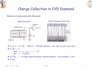
Charge Multiplication • At high fluences and bias voltages, charge multiplication of the signal in the detector has been observed • Signal is multiplied through the process of impact ionization • Impact ionization in silicon begins when the electric field reaches 10-15 V/μm • Charge multiplication can be beneficial for sensors, leading to higher signal • Same process that is responsible for charge multiplication also leads to increased noise and lower breakdown voltage [I. Mandic, 12th RD50 workshop, 2008] C. Betancourt, 23rd RD50 Workshop, CERN
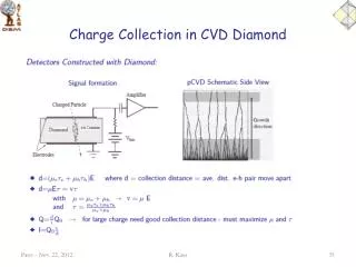
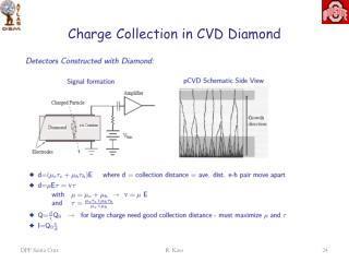
Charge Multiplication Detectors • CERN RD50 investigating rad-hard detector designs, with one option being charge multiplication detectors • 1 cm x 1 cm, n-in-p FZ strip detectors developed by MICRON • 5 type of wafers were produced: standard, double diff. time, double implant energy, thick and thin • Sensors of various strip width (w) and pitch (p) were produced, as well as sensors with floating (f) and biased (i) intermediate strips between readout strips • Detectors aim to enhance the electric field near the readout strips • Sensors irradiated with protons (Karlsruhe) or neutrons (Ljubljana) 0 10 y [μm] 20 2×10⁵ 30 1×10⁵ 0 100 120 140 160 180 200 220 x [μm] [L. Atlan, 20th RD50 workshop, 2012] C. Betancourt, 23rd RD50 Workshop, CERN
ALIBAVA Readout System • Charge collection measurements are done through the ALIBAVA readout system • The daughterboard carries 2 analog front-end ASIC (Beetle) chips, which perform amplification and shaping of the signal • The analog signal is sent to the motherboard, controlled by an FPGA, and converted into digital counts using a 10-bit ADC (Analogue to Digital Converter) • The raw data is sent to a PC from the motherboard using a USB connection, and analyzed by custom software based off the ROOT framework C. Betancourt, 23rd RD50 Workshop, CERN
Beta Source Measurements • MIPs from a 90Sr source are used to perform charge collection measurements • Time between trigger signal and edge of a 10 MHz clock is measured by the ALIBAVA TDC • For each event, channel with largest SNR is chosen, and mean is calculated for each 1 ns time bin • Only events in 10 ns window around max are considered • Resulting spectrum is fitted with a convolution of a Gaussian and Landau distribution to determine MPV C. Betancourt, 23rd RD50 Workshop, CERN
Freiburg vs. Liverpool • Compare results of same detector type and fluence • Freiburg and Liverpool show same values • => Results are comparable between different sites C. Betancourt, 23rd RD50 Workshop, CERN
Fluence: 1×10¹⁵ neq/cm2 C. Betancourt, 23rd RD50 Workshop, CERN
Neutron Irradiation: 5×10¹⁵ neq/cm2 • Three wafers (2E imp, thick, extr. diff.) show signs of CM past 600V with no significant increase in noise • Enhancement of charge is small, but consistent among wafer types relative to std for various sensor geometries C. Betancourt, 23rd RD50 Workshop, CERN
Effect of a biased/floating intermediate strip Neutron 5e15 • Detectors with floating intermediate strips show enhanced charge compared to no intermediate strip detectors • Detectors with biased intermediate strips show a deficit of charge compared to no intermediate strip detectors C. Betancourt, 23rd RD50 Workshop, CERN
Neutron 5×10¹⁵ neq/cm2: w/p comparison • CM only seen at Vbias > 600V • Both Extr. Diff. and 2E imp. Show signs of CM with respect to standard wafer • Lower w/p ratio leads to more pronounced multiplication (as expected since fields are larger at strip edges) C. Betancourt, 23rd RD50 Workshop, CERN
Laser Scan Measurements • IR laser is focused on the detector surface with an optical microscope • Laser spot on surface ~ 3 μm • IR photons do not penetrate fully through detector bulk, so that only relative position efficiency measurements can be made • Sensor is held at a constant bias voltage, and the laser is scanned between the aluminum strips C. Betancourt, 23rd RD50 Workshop, CERN
Laser Scan Results Unirradiated std p=80, w=25 Vbias=100 V std p=80, w=25, i=10 Vbias=100 V C. Betancourt, 23rd RD50 Workshop, CERN
Long-term tests (std, p80,w60, 1e15) • Real-world application requires sensors to be operated at high voltages for long time intervals • Initial tests taken over many days indicates degradation of the CM effect • While signal goes down with time, noise increases C. Betancourt, 23rd RD50 Workshop, CERN
Summary • The RD50 collaboration is investigating charge multiplication sensors as a viable option for radiation hard detectors • This study focuses on MICRON strip detectors of various geometries and wafer types • CM observed at 1e15 neq/cm2 for neutron irradiated samples at high bias voltages (>1000 V), while proton irradiated samples show no clear signs of CM • At 5e15 neq/cm2 several sensors (2E imp., extr. diff., thick) show signs of charge multiplication relative to the standard sensor (std p=80, w=25) • Detectors with floating intermediate strips tend to enhance charge collection while detectors with a biased intermediate strip tend to decrease charge collection relative to sensors without intermediate strips • Lower width over pitch ratio (w/p) leads to more charge • Laser measurements can help differentiate different sensor types • Initial long term CC tests indicate degradation of signal in CM mode C. Betancourt, 23rd RD50 Workshop, CERN
Acknowledgements Irradiations supported by the Initiative and Networking Fund of the Helmholtz Association, contract HA-101 (“Physics at the Terascale”) The research leading to these results has received funding from the European Commission under the FP7 Research Infrastructures project AIDA, grant agreement no. 262025 We would like to thank the irradiation teams and Ljubljana and Karlsruhe16 C. Betancourt, 23rd RD50 Workshop, CERN
BACKUP SLIDES C. Betancourt, 23rd RD50 Workshop, CERN
CV-Measurements before Irradiation C. Betancourt, 23rd RD50 Workshop, CERN
Unirradiated Results • Full depletion reached at 100-125V • No charge multiplication observed up to 1100V on any sensor • Large spread of collected charge for sensors from a given wafer, no clear correlation on geometry • Most sensors show no breakdown up to 1100V C. Betancourt, 23rd RD50 Workshop, CERN