Download
1 / 16
160 likes | 250 Vues
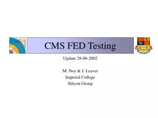
CMS FED Testing. Update 31-05-2002 M. Noy Imperial College Silicon Group. DAC Evaluation board. LVDS. UTP. LVTTL. SEQSI. UTP. VME. Opto-Tx. I2C control. I2C master. Optical Fibre. 8 bit oscilloscope. Coax. Opto-Rx. GPIB. PC. CMS FED Testing. Currently:.

E N D
CMS FED Testing Update 31-05-2002 M. Noy Imperial College Silicon Group
DAC Evaluation board LVDS UTP LVTTL SEQSI UTP VME Opto-Tx I2C control I2C master Optical Fibre 8 bit oscilloscope Coax Opto-Rx GPIB PC CMS FED Testing Currently: Line driver + (optional) level shift LVDSLVTTL I2C slave Network
CMS FED Testing Picture of the DAC evaluation board DAC Line driver LVTTL data in, from level converter UTP out
CMS FED Testing Picture of the key link components UTP from DAC/line driver Optical fibre Opto-Tx Opto-Rx Single ended output to scope I2C cable
10111011010 1 scope CMS FED Testing Opto-Tx DAC Evaluation Board Line driver UTP DAC UTP Opto-Rx Vout
CMS FED Testing Signal before the link 200mV (V+-V- =400mV) differential signal with no offset. higher bandwidth ringing and faster rise/fall time. Time scale is relative to the scope trigger point on all plots.
CMS FED Testing Signal after the link Single ended, with offset. No ringing but slower rise/fall times
CMS FED Testing Signal noise/jitter after the link Note:no scale on the width of the line. This is an impression of the infinite persistence scope trace => spread unknown. (Measurements are real).
CMS FED Testing Rise time, 10% to 90% of full scale.
CMS FED Testing Fall time 90% to 10% of full scale
CMS FED Testing Linearity: link is being operated in the linear region of the Tx/Rx Settings: x0, x1, x2, x3, x4, x5=0,0,0,0,1 (recommended by CERN) 000 01
CMS FED Testing Sample APV25 pair of multiplexed frames with simulated 1 MIP signal
CMS FED Testing Multiplexed APV25 header with zero pipeline address 2 error bits pipeline address (16 bits) 2x12x25ns bits = 6 start bits
CMS FED Testing Zoom in of the 1 MIP signal upon its pedestal • Approx: • Pedestal value here is 509 lsbs, 4096 levels in 405mV0.099mV/lsb • 1 MIP 4096/8=512 lsbs • Total signal =570+(405/4096)*(509+512)=570+0.099*1021=671mV
CMS FED Testing Summary Have a complete working single fibre, possible to drive 4 with identical signals using the current Opto-Tx. Possible to obtain a further 2 of the 4 channel prototypes from CERN complete 12 channels could in principle be driven with identical signals. Work is in progress to produce an application specific version of the SEQSI simpler operation longer RAM pipeline clean/synchronous stop from VME possible stepping through
CMS FED Testing Future Work Have 1 (untested) Opto-Rx emulator to drive the analogue stage of the FED directly over copper (I.e. eliminating the optical link) Temperature: have observed significant temperature variation of the signal =>Define the laser temperature stability requirements for testing Verify DAC Linearity: Summer student More thought into a test vectors and their comparison with the FED output