Download
1 / 10
100 likes | 212 Vues
CMS Tracker FED Front End Module Analogue Circuit Considerations. Draft 1.0 Rob Halsall et al. Signal Ranges. Opto RX Output. ADC Input. 1.56 V. 1.5 V. 1.4 V. Common Mode. 0.5 V. 0.4 V. Opto RX Offset, 0.2V -> 0.56V. 0.2 V. 0 V. 0 V.

E N D
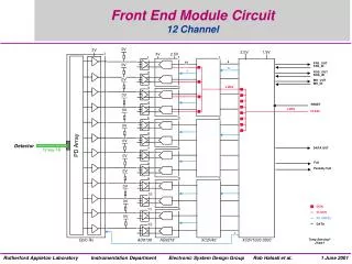
CMS Tracker FED Front End Module Analogue Circuit Considerations Draft 1.0 Rob Halsall et al.
Signal Ranges Opto RX Output ADC Input 1.56 V 1.5 V 1.4 V Common Mode 0.5 V 0.4 V Opto RX Offset, 0.2V -> 0.56V 0.2 V 0 V 0 V Limits of Opto Rx Output, assuming default opto settings - see below 1V range of header/signal + common mode -> 10 bit, 1 mV/bit 0.25V range of signal -> 8 bit, 1mV/bit Assume Opto Rx Offset voltage closely matched across all 12 channels Default Opto Rx Controls = 000110
Single Stage AD8138 or equivalent High AC current fed back to Opto Rx Output DC Currents effecting operating point Opto Rx ouput is a current source not voltage source External resistor diff gain of 2 Gain is adjustable 2V peak to peak mode 1500R VD=+3.3V +3.3/5V Opto Rx 8138 750R + - 22R + 10 ADC 100R 750R - + 22R - -3.3/5V VD 1500R VD/3 DAC High AC currents fed back through feedback resistors Causes Ripple Problem - couples directly to output Point needs less than half LSB ripple ~500µV Common to up to 12 channels in module Possible cross talk between channels
Single Stage AD8131 or equivalent High AC current fed back to Opto Rx Output DC Currents effecting operating point Opto Rx ouput is a current source not voltage source External resistor-less diff gain of 2 2V peak to peak mode VD=+3.3V +3.3/5V Opto Rx 8131 + - 22R + 10 ADC 100R - + 22R - -3.3/5V VD VD/3 DAC Ripple Problem - couples directly to output Point needs less than half LSB ripple ~500µV High AC currents fed back through feedback resistors Common to up to 12 channels in module Possible cross talk between channels
Two Stage AD8138-8131 or equivalents Vout+ = Vin+ Vout- = 2 VOCM - Vin+ Vout+ = VOCM + Vin+ Vout- = VOCM - Vin+ Resistor-less gain of -1 External resistor-less gain of 2 2V peak to peak mode VD=+3.3V +3.3/5V +3.3/5V 8138 8131 - + + - 22R + 10 ADC Opto Rx + - - + 22R - -3.3/5V -3.3/5V 100R VD VD/3 DAC Driving High Impedance Inputs Common to 12 channels in module
Two stage transfer functions example AD8131 AD8138 Opto Rx Output Offset of 0.2V Signal swing of 1V ADC in 2 VPP Mode ADC Common Mode VDD/3 = 1V
Single Stage EL2140 or equivalent External resistor- less gain of 2 2V peak to peak mode VD=+3.3V +3.3V Opto Rx 2140 + + 22R + 10 ADC 100R - - 22R - -3.3V VD VD/3 True Differential Instrumentation Amplifier 3 op-amp internal architecture - to be confirmed All Inputs High Impedance DAC Driving High Impedance Inputs Common to 12 channels in module
Summary AD8131/8AD8131 & 8EL2140C Approach 1 stage 2 Stage 1 Stage Amp type Diff Diff Diff Instr Amp Gain Adj Yes/No No No Ripple >= LSB <<LSB <<LSB Power Estimate* 85W 95W 75W Cost Low/Mod High Low Vendor Major Major Intersil Second Source TI TI No? Package µSOIC µSOIC SOIC Sim Model Yes Yes Yes EL2140C - needs further study? * Estimated FED Power - still under study
9U Board LayoutFront End Envelope 130 mm 270 mm 1 45 mm 366.7 mm 8
Front End Module LayoutEL2140/XC2V40/XC2V2000 27 x 27 mm FPGA XC2V1000- XC2V3000 FG676 33 x 40 mm Opto Rx NGK 45 mm 12 x 12mm FPGA XC2V40 CS144 9 x 9 mm ADC AD9218 ST48 130 mm 5 x 3 mm DIFF OP-AMP AD9218 RM8 - µSOIC N.B. No Passives Shown DIFF OP-AMP EL2140 SOIC 5 x 6 mm 17 x 17mm FPGA XC2V250 FG256 Double Sided Single Sided