Download
1 / 16
160 likes | 173 Vues
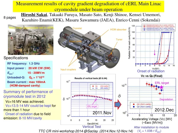
Hiroshi Sakai , Takaaki Furuya, Masato Sato, Kenji Shinoe, Kensei Umemori, Kazuhiro Enami(KEK), Masaru Sawamura (JAEA), Enrico Cenni (Sokendai). 8 pages. Main linac cryomodule set in cERL. Cryostat. HOM absorber. Tuner. 9-cell cavity.

E N D
Hiroshi Sakai, Takaaki Furuya, Masato Sato, Kenji Shinoe, Kensei Umemori, Kazuhiro Enami(KEK), Masaru Sawamura (JAEA), Enrico Cenni (Sokendai) 8 pages Main linac cryomodule set in cERL Cryostat HOM absorber Tuner 9-cell cavity Measurement results of cavity gradient degradiation of cERL Main Linac cryomodule under beam operation Specifications RF frequency: 1.3 GHz Input power : 20 kW CW (SW) Eacc: 15 - 20MV/m Unloaded-Q:Q0 > 1*1010 Beam current : max 100mA (HOM-damped cavity) Input couplers Onset of radiation ERL target Summary of performance of cryomodule test in 2012 Vc=16 MV was achieved. Vc=13.5-14 MV could be kept for more than 1 hour Onset of radiation due to field emission: 8-10 MV/cavity Degradation 2012.Dec 2011.Nov Vertical Test 1 After installation to module (Vc = 1.038Eacc) TTC CR mini-workshop 2014 @Saclay. (2014.Nov.12-Nov.14)
Target and status of Compact ERL (cERL) in 2013& 2014 • Due to the large field emission, we set the beam energy to 20MeV • Energy:20MeV(ML:16.7MeV(8.36MV+8.36MV)+Inj 3.3MeV) • Beam current:1.3GHz 10uAcurrent (CW) with Energy recovoery Initial target of cERL NEG coating chamber Magnet setting & alignment Injector beam commissioning 5.5MeV Vacuum chamber setting Cool down aging Cool down to 2K Beam commissioning (5/22 – 6/20) Beam commissioning (1/30 – 3/14) Return loop beam comissining(12/16-12/20) History of cooling (2013.Nov.-Dec.) cERLreturn loop commisisioning Keep 3K/h(avoid HOM damper crakcking) Upper ML cavity temp Lower ML cavity temp High power test (total:injector & ML) High power test (each cavity ) 2K LBP :Upper HOMdamper temp SBP : Middle HOM damper temp LBP : Lower HOM damper temp 1 week Normal operation of beam and/or high power test start cooling (9:00~12:00)to 2K。13:00~22:00(or24:00),2Kkeep&study, midnight & weekend 4K keep
When we shorten the gate width to 10us, we could not see the field emission. First beam operation in 2013 Dec.(Screen shot of field emission and this effect) Profile of field emission Screen shot of field emission of 8.3MV of ML1 & 8.3MV of ML2 8.3MV with gate width of 100ms of CCD camera. We could see the profile of field emission. screen e- beam 20MeV Main linac cryomodule Beam profile We could acceralate the beam without HOM damper effect and/or coupler kick. No field emission effect was observed during beam operaion. After that, we could see the beam profile without field emission effect with 10us gate width of CCD.
What happened during long term beam operation to cavities (radiation & cavity performance) We set two types of radiation monitor. (radiation monitor (ALOKA), PIN profile monitor) near the beam axis. Radiation measurement during beam operation with 20MeV for 3 weeks. We found sudden jump after 2weeks operation. No6 Radiation monitor #4 cavity(upper) ML1 No5 Radiation monitor #3 cavity(lower)ML2 Keep 8.57MV of each cavity every daytime 1week Increase radiation(No.6) e- Radiation (mSv/h) No.5 16 PINdiodes Q degradation & change of PIN diodes Lower cavity 16 PIN diodes We met Q degradation during beam operation. PIN profile were also increased totally. Same timing response Fatal Q decrease like crack of Hom damper was observed 2013.Dec.12 (same as 2012.Dec.) Operation voltage Lower PIN Vc=10MV Upper PIN Cavity voltage Decrease Q0 during operation No6 2012.Dec. No5 Upper PIN 2014.Mar.10 Lower PIN 2014.Feb—Mar. Vc=10MV 1hour
Pulse processing ML1 Vc Apply pulse processing During beam operation, we apply pulse processing in order to eliminate the field emission source by applying high field. Measured voltage(digital)(Vc) Sudden high peak 1hour 100ms Pulse processing Vc Base:8.57MV Upper PIN diode Duty 10Hz 4ms [peak:11MV] (pulse) QL ~ 1*10^7 t ½ = 1ms , 4ms is larger t ½ When we applied pulse processing, we could see the decreasing of PIN signal individually. pulse processing works well Pulse processing applied(10Hz 4ms) 8.5MV+2.5MV(pulse) ML1:15min+ 1hour ML2:15min+ 1hour Pulse processing was effective for both cavities. (ML1: 8.57MV & ML2:8.57MV) Upper radiation(No.5) 38.7mSv/h (2/25 21:00) 20.48mSv/h (2/26 21:47) Lower radaition(No.6) 133mSv/h (2/25 21:00) 77.9mSv/h (2/26 21:47) Radiation reduced to half by pulse processing. Now pulse agingworks for reducing field emission during beam operation. We plan to try He processing end of beam operation (first try at V.T)
DA/A ~ 0.02% DF ~ 0.02deg Cavity performance under beam operation of cERL (2014.Jan-Jun.) FPGA Virtex5-FX ML2 Vc ML1 Vc 8 hours 8 hours Piezo voltage uTCA 1kHz piezo ML1 vac ML2 vac Microphinics pk-pk = 7Hz Piezo feedback works well He return gas (52W:static+inj+ML) Normal decay time~ 1ms オシロの絵(trip) Pt : yellow 8 hours Very fast He pressure (3kPa+-10Pa) He level 50us We operated from 13:00-22:00 under 2K cooling. Vc keep 8.57MV for 2 cavities. 1 trip (burst) was usually observed (Pref ITL). We have enough cooling power and keep to 2K stably with injector & main linac by cryogenic
Present status (May to June 2014) Operation Vc Operation Vc During beam operation During beam operation Q0 values were measured by He gas flow ratio by keeping CW field.We met Q degradation during beam operation. But we keep same performance within error bars after degradation from May to June in 2014 by trying pulse processing every 2 weeks. We continue to see the cavity performance on next beam operation.
Summary • We met the Q degradation & radiation increase during beam operation. • We can reduce pulse processing pragmatically. • In beam operation, we kept stable operation by using digital feedback system. • Several trips were observed on a half year. • Now we keep stoping the cavity degradiation by using several pulse processing. And we will try He processing to much reduce the field emission source. • We continue to see the cavity performance on next beam operation.
30kWIOT 16kW Solid State AMp Setup of high power test at cERL Radiation sensor (下流) #4 cavity(upper) Radiation sensor (上流) #3 cavity(lower) QL : 1.31*10^7(上流decay) 1.01*10^7(下流,decay) 場所は少し違う PIN radiation profile monitor set around beam axis Si PIN diode set around beam axis 16 Si PIN diodes at each position #3 cavity(lower) #4 cavity(upper) SBP side LBP3 LBP4 SBP3 SBP4 LBP side 2012年から設置しており、これで前回の放射線の比較を行う。
Digital LLRFによる空洞安定性(total 20MeV時の安定性) FPGA Virtex5-FX 入射 空洞 主空洞
今回は1側から覗いた。 4or8が精度が出にくい。 冷却中の主空洞Alignment 冷凍機側0.2-0.5mm (ここがエラーがでかい) h 1-4 入力カプラー側 0.7mm h 5-8 2012年の冷却時の 変化のデータ 下側1.0mm v 1-4 下側0.2mm 途中ずれたか? 大体前回を再現している。 v 5-8 空洞中心の変化は0.4mm程度
Next case (6/12) 79mSv/h 250mSv/h 400mSv/h (final)(upper cavity)
ML1 Pulse aging (6/14) ML2 pulse aging start Vc = 8.6MV+1.9MV (4ms,10Hz, pulse) ALOKA ML1 0:29 ML1 : Vc=0MV ML2 Vc=8.57MV GV close ALOKA No5 459 mSV/h, No6 204mSv/h 2:22 ML1 Vc=0MV ML2 Vc=8.57MV GV close ALOKA NO5 1.31mSv/h (much reduce) ALOKA No6 111.4mSv/h (half)
Ring 16 PIN diodes were set on both jacket sides to compare the radiation profile with rotating mapping Typical example of chaging How to know the profile and radiation source on cryomodule test ? #4 cavity before jacket welding for cERL Field emission (F.E) electron run along cavity axis. We think angular distribution of F.E preserved and detected outside of jacket near both end. -mode 22MV/m Q0=8.0*10^9 Q-E curve of 1st #4 cavity V.T Xray onset start 14MV/m Peak at 360° 22MV/m x-ray rotating mapping Broad Peak at 180° Peak at 360° 22MV/m x-ray mapping by both jacket PIN diodes Broad Peak at 180° Radiation profile were detected from both direction by a ring of 16 PIN diodes and agree well with x-ray angular distribution of rotating mapping. 16 PIN can detect radiation profile during cryomodule test.
Sudden burst event was observed under keeping field of 14.5MV After burst Detail radiation profile measurement Before burst #3 (lower) #4 cav #4 (upper ) Field decreased ・Radiation pattern was changed from V.T ・Radiation pattern also changed after X-ray burst ・Another new radiation sources were produced during assembly work and high power test.