Download
1 / 26
260 likes | 335 Vues
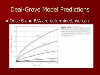
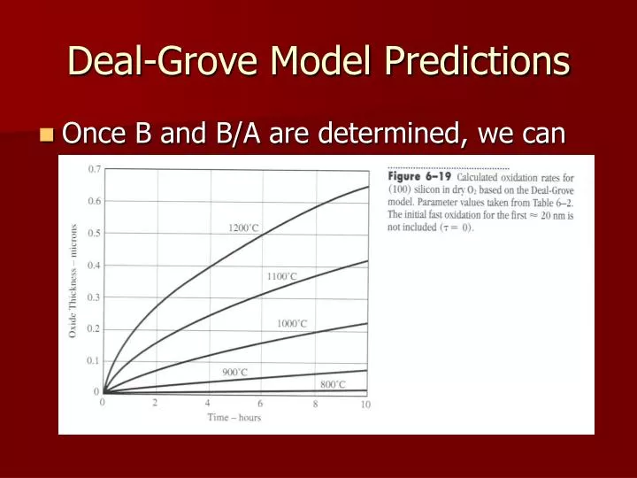
Deal-Grove Model Predictions. Once B and B/A are determined, we can predict the thickness of the oxide versus time. Deal-Grove Model of Oxidation. B. P. 1200 C. Mask thickness ( m m). 1200 C. 1100 C. 1100 C. 1000 C. 900 C. 1000 C. 900 C. Diffusion time (hr).

E N D
Deal-Grove Model Predictions • Once B and B/A are determined, we can predict the thickness of the oxide versus time
B P 1200 C Mask thickness (mm) 1200 C 1100 C 1100 C 1000 C 900 C 1000 C 900 C Diffusion time (hr) Oxide as a Diffusion Barrier • Diffusion of As, B, P, and Sb are orders of magnitude less in oxide than in silicon • Oxide is excellent mask for high-temperature diffusion of impurities 10 10 Boron Phosphorus 1 1 0.1 0.1 0.01 0.01 0.1 0.1 1.0 10 100 1.0 10 100
Other Models • A variety of other models have been suggested, primarily to correct the deficiencies of the Deal-Grove model for thin oxides • These include • The Reisman power law model • The Han and Helms model with parallel oxidation paths • The Ghez and van Meulen model to account for the effect of oxygen pressure • Some of these models do a much better job for thin oxides • None are widely accepted
Other Topics • Several topics other than the simple planar growth of wet and dry oxide are important • These include • Thin oxide growth kinetics • Dependence on oxygen pressure • Dependence on crystal orientation • Mixed ambient growth kinetics • 2D growth kinetics
Example: 2D Growth • There are several interesting observations • There is significant retardation of the oxide growth in sharp corners • The retardation is more pronounced for low temperature oxidation than for high temperature oxidation • Interior (concave) corners show a more pronounces retardation that exterior (convex) corners
Example: 2D Growth • Several physical mechanisms are needed to understand these results • Crystal orientation • Oxidant diffusion • Stress due to volume expansion • Kao et al suggested changes to the linear-parabolic (Deal-Grove) model to correct for these effects • Most of these effects are built into the modeling software such as SUPREM IV and ATHENA
Measurement Methods • The parameters of interest include • Thickness • Dielectric constant and strength • Index of refraction • Defect density • There are three classes of measurement • Physical (usually destructive) • Optical (usually nondestructive) • Electrical (usually nondestructive)
Physical Measurements • Simple step height technique (DekTak) • Etch away oxide with HF • Use a small stylus to measure the resulting step height • The resolution is <10 nm • More complex technique uses one or more of the SFM concepts (AFM, MFM, etc) • Technique has atomic resolution • SEM or TEM (electron microscopy) • All require sample preparation that makes the tests destructive and not easy to use in production
Optical Measurements • Most optical techniques use the concept of measuring reflected monochromatic light • If monochromatic light of wavelength shines on a transparent film of thickness x0, some light is reflected directly and some is reflected from the wafer-film interface • For some wavelengths, the light will be in phase and for others it will be out of phase • constructive and destructive interference • Minima and maxima of intensity are observed as is varied
Color Chart http://www.htelabs.com/appnotes/sio2_color_chart_thermal_silicon_dioxide.htm
Optical Measurements • Instrument from Filmetrics(http://www.filmetrics.com)
Optical Measurements • The positions of the minima and maxima are given bym=1,2,3… for maxima and ½,3/2,5/2,… for minima • This is called reflectometry and works well for thicknesses over a few 10’s of nm
Optical Measurements • If one does not know n, or if the film is very thin, then ellipsometry is better • When multiple wavelengths of light are used, the instrument is known as a spectroscopic ellipsometer
Optical Measurements • Here, one uses polarized light. • The measurement may be performed at multiple angles of incidence to obtain a higher degree of accuracy • One can get the index of refraction as a function of wavelength as well as the extinction coefficient • Can be used to measure thickness to <1 nm • Fitting routines are necessary to take into account rough interfaces between Si and SiO2 layers.
Cauchy Equation Sellmeier Equation
Electrical Measurements • These measure properties that correlate directly to the performance of the devices fabricated using the oxides • The dominant techniques is the C—V measurement • The basic structure for the measurement is the MOS capacitor • The usual combination is Si-SiO2-(Al or pSi) • Any conductor-dielectric-semiconductorcan be used
MOS Capacitor + Al tox V Si wafer Al -
http://www.mtmi.vu.lt/pfk/funkc_dariniai/transistor/mos_capacitors.htmhttp://www.mtmi.vu.lt/pfk/funkc_dariniai/transistor/mos_capacitors.htm
C-V Plot http://ece-www.colorado.edu/~bart/book/book/chapter6/ch6_3.htm#fig6_3_5
C-V Plot • Differences between high frequency and low frequency C-V data • Doping concentration in Si near Si-oxide interface • Voltage shift proportional to charged defects within oxide