Download
1 / 32
320 likes | 492 Vues
COE 1502 MIPS Multicycle CPU Architecture Sequential Logic & Control. MIPS Instruction Set Architecture. Instruction Set Architecture Interface between programmer/user and hardware Instruction set Instruction encoding/representation 6800-series and MIPS are two different ISAs

E N D
COE 1502MIPS Multicycle CPU ArchitectureSequential Logic & Control
MIPS Instruction Set Architecture • Instruction Set Architecture • Interface between programmer/user and hardware • Instruction set • Instruction encoding/representation • 6800-series and MIPS are two different ISAs • 6811 is a one address architecture • Instructions specify one address (accumulator-based) • MIPS is a three address architecture (fixed instruction width) • Instructions specify three addresses (2 operands and 1 destination) • i86 and the IBM 360 is a two address architecture • Execution time = instruction count * cycles/instruction * 1/clock rate
MIPS Instruction Set Architecture • MIPS is a load/store ISA • All operations performed using registers • Operands and results • Data is loaded into registers from memory • Data is stored from registers into memory • MIPS has one addressing mode for load/stores • base-offset • 32-bit indirect (pointer) addresses (set 16-bit offset to 0) • Byte-addressed memory (set base register to 0, use offset)
MIPS Instruction Set Architecture • 32 general purpose integer registers • Some have special purposes • These are the only registers the programmer can directly use • $0 => constant 0 • $1 => $at (reserved for assembler) • $2,$3 => $v0,$v1 (expression evaluation and results of a function) • $4-$7 => $a0-$a3 (arguments 1-4) • $8-$15 => $t0-$t7 (temporary values) • Used when evaluating expressions that contain more than two operands (partial solutions) • Not preserved across function calls • $16-$23 => $s0->$s7 (for local variables, preserved across function calls) • $24, $25 => $t8, $t9 (more temps) • $26,$27 => $k0, $k1 (reserved for OS kernel) • $28 => $gp (pointer to global area) • $29 => $sp (stack pointer) • $30 => $fp (frame pointer) • $31 => $ra (return address, for branch-and-links) • Program counter (PC) contains address of next instruction to be executed
MIPS Instruction Set Architecture • There are several distinct “classes” of instructions • Arithmetic/logical/shift/comparison • Load/store • Branch • Jump • There are three instruction formats (encoding) • R-type (6-bit opcode, 5-bit rs, 5-bit rt, 5-bit rd, 5-bit shamt, 6-bit function code) • I-type (6-bit opcode, 5-bit rs, 5-bit rt, 16-bit immediate) • J-type (6-bit opcode, 26-bit pseudodirect address)
Multicycle CPU Design • You are to design a multicycle CPU that implements the instruction set listed on the webpage • Refer to chapter 5 in the H&P text for design hints • Note: H&P design only includes a subset of the required instructions! • Branch and jump types (including and-link types) • Shift instructions (static and variable) • Halfword- and byte- load and store
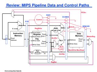
Multicycle CPU Design: Datapaths • A multicycle CPU splits the execution of each instruction into multiple clock cycles • Control unit is FSM • Establishes datapaths for each instruction • A datapath is combinational logic where • Input comes from memory element • Output is latched into a memory element • Data may have to be routed through a multiplexor • May be represented with register transfer language • Components needed (from COELib): • 32x32 register file
Multicycle CPU Design • Goal is to balance the latency of the operations performed during each clock cycle • At most one of the following can occur within one clock cycle: • One ALU operation • One register file access (1 write and 2 reads) • One memory access • Actually will take multiple clock cycles before we get a cache • Our execution stages will be separated into 5 cycles • Instruction fetch • Fetch new instruction from memory, compute next PC value • Performed for all instructions • Decode • Fetch register values from register file, compute branch address • Performed for all instructions • Execute • Perform A/L/S operation for A/L/S R and I-type instructions • Compute address for load and store instructions • Determine if branch is taken for branch instructions • Jump for jump instructions • Link for branch-and-link and jump-and-link instructions • Memory • Access memory for load and store instructions (skip for all others) • Write back • Write register result back to register file for A/L/S/load instructions (skip for all others)
Example • Consider execution for R-type A/L/S instruction… • Cycle one (FETCH) • IR <= Memory[(PC)] • PC <= (PC)+4 • Cycle two (DECODE) • ALUOUT <= PC + SignExtend((IR(15..0))*4) • A <= RegFile(IR(25..21)) • B <= RegFile(IR(20..16))
Example • Cycle three (EXECUTE) • ALUOUT <= ALUOp(A, B, IR(10..6), IR(31..26), IR(5..0)) • Perform ALU operation • Cycle four (WB) • RegFile(IR(15..11)) <= ALUOUT • Write back result
Example • Consider execution for load instruction… • Cycle one (FETCH) • IR <= Memory[(PC)] • Fetch instruction • PC <= (PC)+4 • Update PC • Cycle two (DECODE) • ALUOUT <= PC + SignExtend((IR(15..0))*4) • Compute branch target, in case this is a branch instruction • A <= RegFile(IR(25..21)) • B <= RegFile(IR(20..16)) • Decode register values
Example • Cycle three (EXECUTE) • ALUOUT <= A + SignExtend(IR(15..0)) • Base+offset computation • Cycle four (MEMORY) • MDR <= Memory(ALUOUT) • Load data from memory
Example • Cycle five (WB) • RegFile(IR(25..21)) <= MDR • Write back memory data to register file
Memory Interface • For this design, assume that there is an external memory for instructions and data • Memory interface • Outputs • MemoryAddress, MemoryDataOut, MemRead, MemWrite • Inputs • MemDataIn, MemWait • Protocol:
Adding Control to your CPU • We need… • A way to assign control states for each cycle of instruction execution • Establish data paths • The control state sequence is different for each instruction • Answer: • State machine
Sequential Logic • Combinational logic • Output = f (input) • Sequential logic • Output = f (input, input history) • Involves use of memory elements • Registers
Target Fire = no Standby Fire=no Finite State Machines • FSMs are made up of: • input set • output set • states (one is start state) • transitions • FSMs are used for controllers No missile detected No locked on missile detected miss hit Locked on Launch Fire= yes Input alphabet {missile detected, locked on, hit, miss } Output alphabet{fire}
Finite State Machines • Registers • Hold current state value • Output logic • Encodes output of state machine • Moore-style • Output = f(current state) • Output values associated with states • Mealy-style • Output = f(current state, input) • Output values associated with state transitions • Outputs asynchronous • Next-state logic • Encodes transitions from each state • Next state = f(current state, input) • Synchronous state machines transition on clock edge • RESET signal to return to start state (“sanity state”) • Note that state machines are triggered out-of-phase from the input and any memory elements they control Combinational logic
Example • Design a coke machine controller • Releases a coke after 35 cents entered • Accepts nickels, dimes, and quarters, returns change • Inputs • Driven for 1 clock cycle while coin is entered • COIN = { 00 for none, 01 for nickel, 10 for dime, 11 for quarter} • Outputs • Driven for 1 clock cycle • RELEASE = { 1 for release coke } • CHANGE releases change, encoded as COIN input
Example • We’ll design this controller as a state diagram view in FPGA Advantage Add new state (First is start state) Add new hierarchical state Note: transitions into and out of a hierarchical state are implicitly ANDed with the internal entrance and exit conditions Add new transition
Example • Go to state diagram properties to setup the state machine…
Example • Specify the output values for each state in the state properties
Example • Specify the transition conditions and priority in the transition properties
Example • Let’s take a look at the VHDL for the FSM • Enumerated type: STATE_TYPE for states • Internal signals, current_state and next_state • clocked process handles reset and state changes • nextstate process assigns next_state from current_state and inputs • Implements next state logic • Syntax is case statement • output process assigns output signals from current_state • Might also use inputs here
Code FSM Architecture ARCHITECTURE fsm OF coke IS -- Architecture Declarations TYPE STATE_TYPE IS ( standby, e5, e10, e25, e30, e15, e20, e35, e50, e40, e55, e45 ); -- Declare current and next state signals SIGNAL current_state : STATE_TYPE ; SIGNAL next_state : STATE_TYPE ;
Clocked Process ---------------------------------------------------------------------------- clocked : PROCESS( clk, rst ) ---------------------------------------------------------------------------- BEGIN IF (rst = '1') THEN current_state <= standby; -- Reset Values ELSIF (clk'EVENT AND clk = '1') THEN current_state <= next_state; -- Default Assignment To Internals END IF; END PROCESS clocked;
Nextstate Process ---------------------------------------------------------------------------- nextstate : PROCESS ( coin, current_state ) ---------------------------------------------------------------------------- BEGIN CASE current_state IS WHEN standby => IF (coin = "01") THEN next_state <= e5; ELSIF (coin = "10") THEN next_state <= e10; ELSIF (coin = "11") THEN next_state <= e25; ELSE next_state <= standby; END IF; WHEN e5 => IF (coin = "10") THEN next_state <= e15; ELSIF (coin = "11") THEN next_state <= e30; ELSIF (coin = "01") THEN next_state <= e10; ELSE next_state <= e5; END IF; WHEN e10 => …
Output Process ---------------------------------------------------------------------------- output : PROCESS ( current_state ) ---------------------------------------------------------------------------- BEGIN -- Default Assignment change <= "00"; release <= '0'; -- Default Assignment To Internals -- Combined Actions CASE current_state IS WHEN standby => change <= "00" ; release <= '0' ; WHEN e5 => change <= "00" ; release <= '0' ; WHEN e10 => change <= "00" ; release <= '0' ; WHEN e25 => change <= "00" ; release <= '0' ; WHEN e30 => change <= "00" ; release <= '0' ; WHEN e15 => change <= "00" ; release <= '0' ; …
Hierarchical States hstate1