The Zener Diode
170 likes | 693 Vues
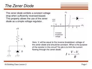
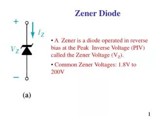
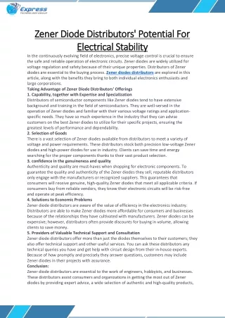
The Zener Diode. +I F. The zener diode exhibits a constant voltage drop when sufficiently reversed-biased. This property allows the use of the zener diode as a simple voltage regulator. zener point. -6. -3. +V F. 1. 2. 3. +V. Constant breakdown voltage. R.

The Zener Diode
E N D
Presentation Transcript
The Zener Diode +IF The zener diode exhibits a constant voltage drop when sufficiently reversed-biased. This property allows the use of the zener diode as a simple voltage regulator. zener point -6 -3 +VF 1 2 3 +V Constant breakdown voltage R Here, Vr will be equal to the reverse breakdown voltage of the zener diode and should be constant. What is the purpose of the resistor in this circuit? Its job is to limit the current flowing through the zener diode: Vr D Kit Building Class Lesson 3
The Bipolar Junction Transistor The transistor is a versatile device usually configured to perform as a switch or as an amplifier. The bipolar junction transistor (BJT) is the most common type and has three leads: 3 3 Collector Collector 2 2 Base Base Emitter 1 Emitter 1 NPN Transistor PNP Transistor In a transistor, the flow of current from the collector to the emitter is controlled by the amount of current flowing into the base of the transistor. If no current flows into the base, no current will flow from the collector to the emitter (it acts like an open switch). If current flows into the base, then a proportional amount of current flows from the collector to the emitter (somewhat like a closed switch). Kit Building Class Lesson 3
The NPN Transistor c c Rb Rb b b + IC + e e + + - - Re Re - - IB Current now flows through the transistor from base to emitter. This causes the transistor to allow current to flow from the collector to the emitter. The size of the collector current depends on the size of the base current and the beta b of the transistor: No current flows from base to emitter, so the transistor acts like an open switch and no current flows from collector to emitter. (Note: current never flows from base to collector or vice versa, regardless of the base current.) A typical transistor has a beta of about 100. Kit Building Class Lesson 3
Base and Collector Currents What’s the base current IB? Use Kirchhoff’s voltage law: c RB b IC + E e - RE 0.7 volts is lost at the junction of the base and emitter IB What’s the maximum value for the collector current? Now find the collector current IC: Kit Building Class Lesson 3
+ - The PNP Transistor c Rb b Ic e Ib Re The PNP transistor behaves identically to the NPN transistor, except that all polarities are reversed. The voltages are applied with opposite polarity, and the currents run opposite to those in the NPN transistor, but all other behaviors are the same. Kit Building Class Lesson 3
The SW+ Transmit Switch to transmit circuit C111 With the key open, Q3’s base and emitter are at the same potential, and no current flows from emitter to base. Therefore, no collector current flows. key (J3) R21 Q3 1 3 10K R20 22K D13 circuit copyright 1998 Dave Benson NN1G V in (12-15V) Closing the key allows current to flow through R20 and R21. The voltage drop across R20 lowers the potential at the base of Q3 and current flows from emitter to base. This also turns on the transistor and allows a collector current to flow. The collector current is fed to the transmit circuit, turning it on. R20 and R21 form a voltage divider to provide the correct bias voltage to the base. With the switch closed, what is the voltage at the base of Q3? Kit Building Class Lesson 3
Mixers In radios, a mixer is a device which is used to shift the frequency of a signal. It does so by multiplying the signal with another carefully-chosen frequency: mixer The output of a mixer is a signal which is a combination of two frequencies: F1+F2, and F1-F2. In reality, other frequencies are also present at the output, due to distortion. All the unwanted frequencies need to be filtered out. output (F) Input (F1) local oscillator (F2) The SW+ has three mixers: two in the receiver and one in the transmitter. In the receiver, the received 7 MHz signal is mixed with 3 MHz from the VFO to get the 4 MHz intermediate frequency (IF). The IF is further mixed with the beat frequency oscillator (BFO) to get audio frequencies out. In the transmitter, the VFO is mixed with a 4 MHz signal to get the 7 MHz output. Kit Building Class Lesson 3
Mixing Two Signals Here, V1 and V2 are the voltages of two signals (sine waves), and they are plotted versus time t. V1’s frequency is 30 Hz and V2’s frequency is 40 Hz. The third line on the graph is V1 times V2, and it has a frequency which is higher than both V1 and V2. Can you see from the graph what the frequency is? It’s easy to see the sum frequency, but can you see the difference frequency in the signal? Kit Building Class Lesson 3
The NE602 Mixer Chip The NE602 mixer chip (or the SA602, NE612, or SA612, which are all essentially identical) is a low-cost solution for mixing needs and is often used in kits. In order to produce an output at pins 4 and 5, three things are required: 1) A supply voltage Vcc which is well-regulated, between 4.5 and 8 volts 2) An input (this is the signal whose frequency is to be shifted) 3) An oscillator to provide a signal to mix with the input. The NE602 has built-in circuitry for providing the oscillator input, requiring only the addition of a few parts which determine its frequency. Kit Building Class Lesson 3
Inputs to the NE602 V+ (9 to 18V DC) The input signal can be unbalanced, as shown here (either pin 1 or 2 can be used). The input signal should be small (less than 180 mV peak-to-peak). 1 NE602 RF input 1K 2 1 mF 6.8V 8 NE602 1 NE602 RF input 3 2 Pin 8 powers the NE602. It requires from 4.5 to 8V DC. The above configuration provides a regulated 6.8V input. The 1K resistor serves to limit current, while the capacitor provides a path to ground for any AC. Pin 3 is the chip’s ground. The input signal can also be applied in a balanced configuration. Here a transformer is used, and it is chosen such that it provides a match to the 1500-ohm input impedance of the NE602. Other configurations might add a capacitor across pins 1 and 2 in order to form a tuned circuit, passing only the frequencies of interest. Kit Building Class Lesson 3
The NE602 Oscillator NE602 6 7 Remember our simple oscillator circuit from Lesson 2? Here it is again--a tank circuit with an amplifier to amplify and reinject a part of the signal to keep the oscillator going. The NE602 provides the amplifier internally. To use its internal oscillator, all that’s required is to connect a suitable tuned circuit across pins 6 and 7. Alternatively, if we want to use our own oscillator, its output should be connect to pin 6, with pin 7 unconnected, and the input level should be between 200 and 300 mV. Kit Building Class Lesson 3
NE602 Oscillator Circuits NE602 6 NE602 6 C1 7 C1 7 C2 Y C2 Y L Here, an inductor has been added in series with the crystal. This has the effect of increasing the inductance of the circuit, which causes the resonant frequency to decrease. This is known as pulling the crystal--getting it to chance its oscillation frequency a bit. What would happen if we replaced the inductor with another capacitor? Here, a crystal is used to set the oscillator frequency. Crystals can be thought of has having both internal inductance and capacitance, and these set the frequency of the crystal. C1 and C2 form the feedback network for the oscillator. Kit Building Class Lesson 3
The NE602 Outputs Pins 4 and 5 of the NE602 are the outputs. The signals from each pin are identical but of opposite phase (pin 4 is negative when pin 5 is positive, and vice versa). Either or both pins can be used for output. 4 4 NE602 use either pin for RF out NE602 RF out 5 5 Here, both pins are used for output. Since they are of opposite phase, the voltage between them is twice the voltage of either with respect to ground. The transformer is used to transform the impedance for the next stage of the circuit. Capacitors could be placed in parallel with either side of the transformer to form tuned circuits to act as a bandpass filter. This is an example of an unbalanced output. Only one of the two pins is used--the other is left unconnected. Kit Building Class Lesson 3
The SW+ Transmit Mixer V in (12 to 15V) from transmit switch The transmit mixer in the SW+ mixes the VFO output with the output from a crystal oscillator using the NE602’s internal oscillator. Here, mixing only occurs when the key is closed. R19 1K 0.01 mF D11 7.6V C109 8 NE602 from VFO 2 4 0.01 to bandpass filter 1 3 5 The desired output from the mixer is the VFO frequency plus the crystal oscillator frequency (about 7 MHz). The outputs are passed through a bandpass filter to get rid of unwanted frequencies. The tuned circuit connected to the NE602 uses a 4.00 MHz crystal for its main component. The inductor connected with the crystal in series has the effect of lowering the frequency a few hundred hertz. Why is this done? 7 C28 6 C29 160 Y5 47 4.0 MHz RFC2 22 mH circuit copyright 1998 Dave Benson NN1G Kit Building Class Lesson 3
Reasons for problems: poor soldering wrong part installed part installed backward part installed in wrong holes solder bridges (connecting parts which shouldn’t be) bad board traces bad parts Tracking down problems: double check parts placements and values look for missed or bad solder joints and bridges ensure all parts are installed is power applied? Key down? etc. follow voltages from source make sure test equipment is connected correctly and working if you can narrow the problem to one place, suspect the part or the traces on the board Troubleshooting Tips Kit Building Class Lesson 3
Install the following parts (all are in Group 5). Be sure to observe correct orientation for U5, Q3, D11, and C110. U5 & its socket Q3 D11 C28, C29, C108-C111 R19-R21 (note: R21 lays down on the board) RFC2 Y5 J3 J3 wiring harness and jacks (see enclosure instructions) Testing: connect key and tuning pot apply power measure voltage at pin 8 of U5 with key down. What should it be? measure same voltage with key up. What should it be? with key down, use oscilloscope to examine signal on pin 4 or 5 of U5. Do you see RF? What does the signal look like? Why? any signal on pin 4 or 5 with the key up? Construction Kit Building Class Lesson 3