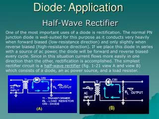
The Gunn Diode
The Gunn Diode. Contents Overview of The Gunn Diode Gunn Effect Two-Valley Model Theory Gunn-Oscillation Gunn Oscillation Modes. Overview of The Gunn Diode. What is it? The Gunn diode is used as local oscillator covering the microwave frequency range of 1 to 100GHz How it works?

The Gunn Diode
E N D
Presentation Transcript
Contents • Overview of The Gunn Diode • Gunn Effect • Two-Valley Model Theory • Gunn-Oscillation • Gunn Oscillation Modes
Overview of The Gunn Diode • What is it? • The Gunn diode is used as local oscillator covering the microwave frequency range of 1 to 100GHz • How it works? • By means of the transferred electron mechanism, it has the negative resistance characteristic • What’s the applications? • Local Oscillator and Avoid Collision Radar instead of Klystron etc.. • What’s the advantages? • Low noise, High frequency operation and Medium RF Power
Negative Resistance In a negative resistance the current and voltage are out of phase by 180. The voltage drop across a negative resistance is negative and a power of -I2R is generated by the power supply. i.e positive resistance absorbs power (passive devices) and negative resistances generates power (active devices).
Microwave Transistors and TEDs Transistors operate with either junctions or gates but TEDs are bulk devices having no junctions or gates. The majority of transistors are fabricated from Si or Ge whereas TEDs are fabricated from GaAs, InP or CdTe.
Contd…… Transistors operate with “warm” electrons whose energy is not much greater than the thermal energy of the electrons in the semiconductors whereas TEDs operate with “hot” electrons whose energy is very much greater than the thermal energy. Because of these fundamental differences, the theory and technology of transistors cannot be applied to TEDs
Gunn Effect • Gunn effect was discovered by J.B Gunn in IBM : 1963 “Above some critical voltage, corresponding to an electric field of 2000~4000 V/cm, the current in every specimen (GaAs) became a fluctuating function of time” Schematic diagram for n-type GaAs diode High-field domain → v = 105 m/s Cathod - + Anode Metal-coated contact
Gunn Effect • (Continue) • The current waveform was produced by applying a voltage pulse of 59V And 10ns duration • Oscillation frequency was 4.5Ghz • The period of oscillation is equal to the transit time of electrons through the device Current fluctuation of N-type GaAs reported by Gunn 0.222ns ≈ 4.5GHz 5ns 10ns
Gunn Effect-Negative Differntial Resistance • Drift velocity of electrons decrease when electric field excess certain value • Threshold electric field about 3000V/cm for n-type GaAs. Drift velocity of electrons in GaAs bulk Vs electric field Drift velocity Negative Differential Resistance 2e7 3 10 Electric field [KV/cm]
Two-Valley Model Theory • According to the energy-band theory of n-type GaAs, there are two valleys in the conduction band • Effective mass of electron is given by: Upper valley (Satellite valley) Lower valley (Central valley) Rate of change of the valley curves slope Central valley Satellite valley K = 0
Two-Valley Model Theory • Effective mass of electron is given by: Rate of change of the valley curves slope • Since the lower valley slope is shaper than the one in upper valley, thus electron effective mass in lower valley is higher than that in upper valley • So that, the mobility of electron in upper valley is less due to the higher effective mass * n-type GaAs
Two-Valley Model Theory • The current density vs E-field according to equation
Two-Valley Model Theory • Negative resistance : the current and voltage of a device are out of phase by 180degree →P = -I2 R • Conductivity of n-type GaAs is given by • The differential resistance of the device is Electron density in lower/upper valley Mobility in lower/upper valley (1)
Two-Valley Model Theory • According to Ohm’s law: • (2) • rewrite equation 2: • (3) • Current density J must decrease with increasing field E • Negative resistance occurs when • (4)
Two-Valley Model Theory • Plot current density vs E-field according to equation (3)
Two-Valley Model Theory According to Ridley-Watkins-Hilsumthoery, the band structure of a semiconductor must satisfy 3 criteria in order to exhibit negative resistance. • The energy difference between two valleys must be several times larger than the thermal energy (KT~0.0259eV) • The energy difference between the valleys must be smaller than the gap energy between the valence and the conduction band. • Electron in lower valley must have a higher mobility and smaller effective mass than that of in upper valley
Gunn-Oscillation (High field domain) • Above Eth, A domain will start to form and drift with the carrier stream. When E increases, drift velocity decreases and diode exhibits negative resistance • If more Vin is applied, the domain will increase and the current will decrease. • A domain will not disappear before reaching the anode unless Vin is dropped below Vth • The formation of a new domain can be prevented by decreasing the E field below Eth
Modes of operation Gunn Oscillation: fL=107 cm/s noL = 1012 cm/s2 Device is unstable because of the cyclic formation of either the accumulation layer or high field domain 2. Stable Amplification: fL=107cm/s noL =1011 cm/s2 to 1012 cm/s2 3. LSA Oscillation: fL >107cm/s Quotient of doping divided by frequency is between 2 x 10⁴ to 2 x 10⁵. 4. Bias-circuit oscillation mode: This mode occurs only when there is either Gunn or LSA oscillation, and it is usually at the region where the product of frequency times length is too small in the figure to appear.
Gunn Oscillation Modes ℇ > ℇth. The high field domain drifts along the specimen until it reaches the anode or until the low-field value drops below the sustaining field ℇsrequuired to maintain Vs as shown in the figure Since the electron drift velocity v varies with E, there are 3 possible modes Transit time domain mode: Oscillation period is equal to transit time efficiency less than 10%. 2. Delayed domain mode: . . Inhibited mode. Low efficiency less than 20%. 3. Quenched domain mode: If E < ℇsdomain collapses before it reaches the anode. When the bias field swings back above the threshold, a new domain is nucleated and the process repeats.Thus oscillation occurs at the frequency of resonant circuit rather than at the transit time frequency. efficiency can reach 13%.
Gunn Oscillation Modes • The Operation in Resonant Circuit 1. Stable domain mode(Without resonant circuit) ℇ > ℇth (Low efficiency less than 10%) 2. Resonant Gunn mode ℇ > ℇs (Low efficiency less than 10%)
Gunn Oscillation Modes 3. Delayed mode : - (High efficiency up to 20%) - There is an ohmic currents higher than domain currents. - fosc is determined by the resonant circuit 4. Quenched mode - (Efficiency up to 13%) - The domain can be quenched before it is collected - So that, fosc is determined by the resonant circuit Positive resistance region The sustaining drift velocity
Gunn Oscillation Modes LSA mode(Limited Space charge Accumulation) (The most efficiency mode more than 20%) The frequency is so high that domains have insufficient time to form while the field is above threshold. As a results, domains do not form. fosc determined by the resonant circuits, is much higher than the transit time frequency
Stable amplification mode When noL < 1012/cm2 the device exhibits amplification at the transit time frequency rather than spontaneous oscillation. This situation occurs because the negative conductance is utilized without domain formation. There are too few carriers for domain formation within the transit time. Therefore amplification of signals near the transit time frequency can be accomplished.
Fabrication Doping density 1.25e17cm-3 Active region : 5e15cm-3 The doping-notch 1e16cm-3 • Structure Electric field T=0 T=3ps Dead zone T=5.6ps T=10ps Distance from the cathode
Summary • Gunn diode is mainly used as a local oscillator covering the microwave frequency range of 1 to 100GHz • By means of the transferred electron mechanism, the negative resistance characteristic can be obtained. This mechanism provides low noise, high frequency operation and Medium RF Power characteristic • The LSA mode is particularly suitable for microwave power generation because of its relatively high efficiency and operating frequency
Reference • “Solid State Electronic Devices”, 3rd Ed, Streetman • “Microwave device & Circuits” 3rd Ed, Samuel Y.Liao