CMOS Logic Gates Design and Layout | CMOS IC Design Flow | CMOS Implementation
180 likes | 550 Vues
Gain an insight on CMOS Design by experts of EssayCorp across the world. We have subject matter experts, who specializes in in VLSI, Logic Gates, PMOS, etc. For any academic help contact us at contact@essaycorp.com<br>

CMOS Logic Gates Design and Layout | CMOS IC Design Flow | CMOS Implementation
E N D
Presentation Transcript
CMOS Design Assignment CMOS Design Assignment (2016) Introduction: Designing a simple CMOS circuit consisting of two-input NOR gate. Schematic of 2-input NOR gate: The schematic shows that there are 2 P-MOS Transistors (Pull up Network) in Parallel and 2 N-MOS Transistors in Series (Pull down Network). When A or B is high inputs, M1 or M2 will be ohmic and the output F will discharge to zero. When both A and B are low inputs, Mp1 or Mp2 will be the output F will charge to Vdd. 1
CMOS Design Assignment Calculations: To calculate W/L)p and W/L)n Lmin=0.2 um, (minimum Feature size) p = * , n, but for optimum delay p n Transistor sizing is chosen in order to minimize propagation delay as minimum as possible. Propagation delay: To Calculate Start from current equation: [( ] And for very small we can neglect this term ( Transistor acts as a resistor ( ) , Kn= ( ) ( Threshold Voltage for N-MOS: Vtn=0.3v, Supply Voltage: Vdd=4v, Minimum Feature size: Lmin=0.2 um, Saturation Voltage: Vdsat=4-0.2=3.8v For =3.5*, Cl=Co=0.5nf Wn=21,Wp=53 Width for N-MOS= 21um Width for P-MOS= 53um 2
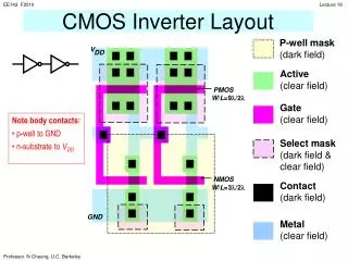
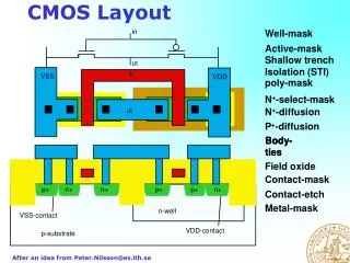
CMOS Design Assignment Layout: 1-Maximum alignment error=0.1 um min routing width >0.1um. By using min routing width=0.2um. 2-Area should be minimized. Metal 1 Metal 2 Poly Diffusion N-Well 3
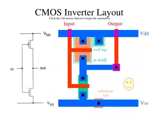
CMOS Design Assignment Explanation: Using Cadence Virtuoso to draw the layout and verify the design rules and the simulations results for 2-input NOR gate. Following these steps to draw the layout: Drawing Transistors To make p and n transistors. For p transistor using n-well and the background in the main layout window will act as your p-substrate. Thus the n transistors is placed directly in the p substrate. However the p transistor will be placed in n-well. Masks used for P transistor: N-well, diffusion, any poly. Masks used for N transistor: P-substrate, diffusion, any poly. Making Connection The next step is to connect the drains of the two N transistors and the first P transistor together to make up the output. The source of the first P transistor is connected to the drain of the second P transistor which is source is connected to Vdd and the source of the two N transistors are connected to Gnd. The two gates of each (N and P) transistor are connected together to form one of the inputs. Metal 1: used for input A, and B. Metal 2: used for output, Vdd, and Gnd. Drawn layers (Masks) used to create a transistor: 1) Well: NMOS are in P-well, PMOS are in N-well 2) Diffusion: defines active vs. isolation regions on layout, and sets Source and Drain for transistor. 3) Poly: gate mask over diffusion mask defines W and L of each transistor. 4) Contact: defines the contacts between the masks. 5) Tap: defines contact to substrate or well. 4
CMOS Design Assignment List of Rules to be Considered: 1) One layer: width, spacing 2) layer to layer: spacing, enclosure, extension, overlap 3) Rules are going to be separated into the masks: N-well, Diffusion, Poly, Contact, and Metal Explanation of Layout: 1) Layout PMOS and NMOS Transistors using calculated Diffusion, Poly and Well Masks. n using p, 2) make input and output ports using metal masks. 3) Connect the masks using Contacts. 4) label the ports and the power lines (VDD and GND). Schematic from Cadence 5
CMOS Design Assignment Waveform Simulations from Cadence A B 0 0 0 1 1 0 1 1 Truth Table for 2-input Nor gate F 1 0 0 0 6