CMOS DYNAMIC LOGIC DESIGN
CMOS DYNAMIC LOGIC DESIGN. Integrated Circuits Spring 2001 Dept. of ECE University of Seoul. Dynamic Logic Motivation. Complementary CMOS Logic V OH =V DD , V OL =GND No Static Power Dissipation For Fan-In of N, (2N) Transistors Required


CMOS DYNAMIC LOGIC DESIGN
E N D
Presentation Transcript
CMOS DYNAMIC LOGIC DESIGN Integrated Circuits Spring 2001 Dept. of ECE University of Seoul
Dynamic Logic Motivation • Complementary CMOS Logic • VOH=VDD, VOL=GND • No Static Power Dissipation • For Fan-In of N, (2N) Transistors Required • Series Network Unavoidable • pseudo-nMOS Logic • For Fan-In of N, (N+1) Transistors Required • Series Network Avoidable • VOLGND • Static Power Dissipation • Dynamic Logic • Combination of Two Design Approaches
PDN Basic Principle – fn Network • CLK=L[PRECHARGE] • MN OFF : Y can’t go down to GND • MP ON : Y prechaged to VDD • CLK=H[EVALUATION] • MP OFF • MN ON • Y can go down to GND • or • stay at VDD • according to PDN evaluation.
PUN Basic Principle – fp Network • CLK=L[PRECHARGE] • MP OFF : Y can’t go up to VDD • MN ON : Y prechaged to GND • CLK=H[EVALUATION] • MN OFF • MP ON • Y can go up to VDD • or • stay at GND • according to PUN evaluation.
fn Network – Operation • EVALUATION PRECHARGE
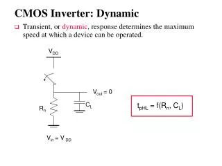
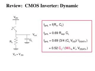
VIL, VIH & VM fn Network – Characteristics • Logic – PDN consists of nMOS Transistors • Number of Transistors: N+2 • Faster Switching Speed due to Reduced # of Transistors • Ratioless Logic: VOH=VDD, VOL=GND • No Static Power Dissipation, Only Dynamic Power Dissipation • Reduced Noise Margin (NML)
fn Network – Example 4-Input NAND Waveform tpHL How about tpLH? tpLH=0!!
fn Network Problem – Leakage Current • ILK = IRD (Reverse-Biased Diode) + IWI (Weak-Inversion) • • For Proper Logic Operation, VDD-DVLK > VIH
Leakage Current Example • ILK= 10nA (for example) • CL= 32.75fF (pp. 133 in textbook) • Leakage Ripple • High Voltage @ Y • VIH for Inverter • VIH=2.92V (pp. 128 in textbook)
fn Network Problem – Charge Sharing • Before A Rising, • After A Rising, • Charge Sharing Ripple
might forward-bias PN junction fn Network Problem – Clock Feedthrough
fn Network Problem – Cascading • Ideally, Y = NOT(X) = NOT(NOT(A)) = A = “H” • Non-Zero Falling Time @ X-node Y-node Also Falling • until X-node reaches VTHN • Basic Problems: Outputs Precharged to VDD & They drives nMOSFET.
DOMINO Logic • Solve Problem of Cascading • But Still Dynamic Logic Leakage, Charge Sharing, Clock Feedthrough • Can’t Make Inverting Logic such as NAND, NOR, … • Very High Speed Operation Achievable
ZIPPER Logic Precharged to VDD (GND) Drives pMOS (nMOS) Logic Speed Unbalance between PDN (nMOS) & PUN (pMOS) Higher Speed Than Domino Due to Lack of Inter-stage Inverters DEC Alpha Processor