Download
1 / 20
420 likes | 1.31k Vues
NEXT GENERATION THIN-FILM SOLAR CELLS. Alison J. Breeze Solexant Corp. San Jose, CA USA. Purpose. Provide overview of basic solar cell characterization measurements Introduce prevalent thin-film solar cell materials and structures

E N D
NEXT GENERATION THIN-FILM SOLAR CELLS Alison J. Breeze Solexant Corp. San Jose, CA USA
Purpose • Provide overview of basic solar cell characterization measurements • Introduce prevalent thin-film solar cell materials and structures • Discussion of key characteristics and challenges for CIGS and CdTe devices
Outline • Basic solar cell characterization • Theoretical efficiency limit and parameters • Overview of leading thin-film solar cell performances • Intrinsic degradation: a-Si vs CIGS and CdTe • Characteristics and challenges • copper indium gallium diselenide (CIGS) • cadmium telluride (CdTe) • Summary
Solar cell characterization:current density – voltage (J-V) curves • Air Mass 1.5 solar spectrum, I = 1000 W/m2 • Open-circuit voltage Voc • Short-circuit current density Jsc • Fill factor: • Power conversion efficiency:
100 80 60 Unscaled Quantum Efficiency (%) 40 20 0 200 300 400 500 600 700 800 900 Wavelength (nm) Solar cell characterization: external quantum efficiency (EQE) • short-circuit • voltage bias F(l) = flux density/unit l EQE for record CdTe device X. Wu, et al, “16.5%-efficient CdS/CdTe polycrystalline thin film solar cell,” Proc. 17th EPSEC, 2001, pp. 995–1000.
0.40 0.30 0.20 Efficiency 0.10 0.00 0.50 1.00 1.50 2.00 2.50 Band Gap / eV Theoretical max h and optimal bandgap • Maximize Jsc: maximize absorption smaller bandgap Eg • Maximize Voc: larger Eg Theoretical maximum h=31% (Shockley-Queisser) under AM1.5 spectra occurs for Eg=1.4eV CIGS CdTe J. Nelson, The Physics of Solar Cells. London: Imperial College Press, 2003, ch. 2, p. 33.
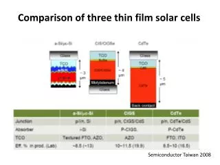
Leading thin-film solar cell technologies • Copper Indium Gallium Diselenide (CIGS, Cu(In1-xGax)Se2) • Cadmium Telluride (CdTe) • Amorphous Silicon (a-Si) Maximum recorded efficiencies* * Martin A. Green, et al, “Solar Cell Efficiency Tables (Version 31),” Prog. Photovolt: Res. Appl., vol. 16, 2008, pp. 61-67.
Intrinsic Initial Degradation: a-Si vs CIGS and CdTe • a-Si suffers from intrinsic degradation, “Staebler- Wronski effect” • connected to amorphous, hydrogenated nature of the material • associated with light exposure • stabilizes after initial drop, ~25% efficiency loss • CIGS and CdTe: small-grained crystalline materials, • not impacted by this type of degradation All solar cells must be encapsulated to protect against environmental effects
CIGS and CdTe device structures CIGS substrate configuration CdTe superstrate configuration
CIGS solar cells Key advantages for CIGS solar cells • tune bandgap 1.04-1.4eV by variation of Ga fraction (increase Ga increase Eg) • direct bandgap absorber with a~105 cm-1 • substrate structure allows for flexible substrates Deposition techniques for CIGS • selenization of precursers with H2Se • sputtered metals reacted with Se gas • evaporation of constituent elements • highest h via three-stage evaporation recipe Deposition techniques for CdS: Chemical bath deposition (CBD) common
Critical Aspects of CIGS Na doping • Critical for high performance devices • promotes CIGS grain growth • passivates grain boundaries to reduce recomination • optimium ~0.1% atomic • diffused from soda lime glass or incorporated separately (ex: NaF) Evaporation: from Cu-rich to Cu-poor • begin with Cu-rich for liquid growth phase • end with Cu-poor for favorable electronic properties Control over constituent ratios: difficult using traditional deposition methods such as co-evaporation
20 18 16 Efficiency (%) 14 12 10 1.0 1.1 1.2 1.3 1.4 1.5 1.6 Bandgap (eV) Uniform variation of Ga/(Ga+In) ratio increase Eg increase Voc (max Eg~1.3eV, Voc~0.8eV) • change primarily in conduction band • optimum efficiency at Eg=1.14eV solar cell theory optimum h decrease at higher Eg from decreased Jsc due to recombination Miguel A. Contreras et al, “Diode Characteristics in State-of-the-Art ZnO/CdS/ Cu(In1-xGax)Se2 Solar Cells,” Prog.Photovolt: Res. Appl., vol.13, 2005, p.209-216
CdS CIGS Mo Ga ratio depth CIGS: Graded Bandgaps Improve performance with graded bandgap across CIGS thickness • Increase Ga and Eg towards Mo interface • Reduce recombination losses • Improve Voc and Jsc • h increase from 13 to 16%* *T. Dullweber et al, “Back surface band gap gradings in Cu(In,Ga)Se2 solar cells,” Thin Solid Films, vol. 387, 2001, pp. 11-13.
100 Std cell 80 1mm cell 60 External QE(%) 40 20 0 400 600 800 1000 1200 Wavelength (nm) Thinner CIGS layers • reduce material usage • and cost • EQE l decrease due to • absorption limitation • Jsc decrease 2-3mA/cm2 • h = 16.9% Kannan Ramanathan et al, “Properties of High Efficiency CIGS Thin-Film Solar Cells,” Proc. 31st IEEE Photovoltaics Specialists Conference, 2005
CdTe solar cells Key advantages for CdTe solar cells • Eg=1.5eV near theoretical optimal value • direct bandgap absorber with a~105 cm-1 • easier to control than quaternary CIGS system Wide range of deposition techniques • Sputtering, close-spaced sublimation, physical vapor deposition, electrodeposition, screen printing • Later processing steps result in similar result for all deposition approaches • CdS: best results with chemical bath deposition
CdS optimization and buffer layer CdS thickness optimization • No photocurrent generated in CdS minimize thickness to maximize transmission to CdTe in blue region (CdS Eg=2.4eV) • Too-thin CdS shunting issue Thin resistivity buffer layer • Transparent Cond. Oxide / buffer / CdS / CdTe / electrode • ex: high resistivity SnO2, In2O3, ZnO, Zn2SnO4
CdCl2 heat treatment for CdTe Heat treatment with CdCl2 required for high Jsc • Methods: • Soak CdTe film in CdCl2:MeOH, heat treat 400°C • Heat treat 400°C in presence of CdCl2 vapor • Effects: • Recrystalization and grain growth in CdTe • Establish or increase CdTe p-type doping • Passivation of grain boundary traps • CdS/CdTe interfacial mixing: CdTeyS1-y/CdSxTe1-x • alleviates structural, electrical defects at interface
Electrode contact to CdTe Key challenge: ohmic contact to CdTe • CdTe valence band 5.7eV • current-limiting Scottky back barrier Simulated dark and light J-V curves: ideal cell (squares) significant series resistance (triangles) significant back contact (circles) M. Gloeckler and J.R. Sites, “Quantum Efficiency of CdTe Solar Cells in Forward Bias,” Proc. 19th EPSE, 2004, pp. 1863-1866
CdTe contact strategies Approaches for non-blocking contact • high workfunction metal or degenerate semiconductor (ex: Au, Sb2Te3, graphite paste) • Formation of p+ doped layer on CdTe surface to promote tunnelling thru barrier • etching to produce p+ Te-rich surface layer • Cu doping • acts as p-type dopant in CdTe • forms Cu2Te (in conjunction with etching) • other dopants (ex: HgTe), included in graphite paste
Conclusions • Basic initial characterizations include J-V and EQE measurements for determining efficiency and utilization of solar spectral range • designing optimal solar cells begins by selecting materials with the right fundamental properties such as band-gap value • State-of-art performance for 3 leading thin-film devices: efficiencies from 9.5% (a-Si) to 19.9% (CIGS) • CIGS and CdTe have been pursued due to their bandgaps, high absorption strengths and other favorable properties, but key challenges remain including bandgap optimization and controlling material profiles (CIGS) and back-contact formation (CdTe)