Chalcopyrite Thin-Film Solar Cells : Present and Future
270 likes | 1.02k Vues
Chalcopyrite Thin-Film Solar Cells : Present and Future. Solar Cell Clean & Regeneratable Energy Source - Sunlight. Wafer vs. Thin-Film Thin-film Solar Cells : Low material consumption, Potential reduction of manufacturing cost. Si Wafer Si thickness : 250-300 μ m. Si Thin-Film

Chalcopyrite Thin-Film Solar Cells : Present and Future
E N D
Presentation Transcript
Chalcopyrite Thin-Film Solar Cells : Present and Future
Solar Cell • Clean & Regeneratable Energy Source - Sunlight
Wafer vs. Thin-Film • Thin-film Solar Cells : • Low material consumption, Potential reduction of manufacturing cost Si Wafer Si thickness : 250-300 μm Si Thin-Film Si thickness : 1-10 μm
Market Status of Thin-Film Solar Cells • Market share of thin-film solar cells decreased to 6.4% in 2005
Materials for Thin-Film Solar Cells • Single Element : a-Si:H, B-doped DLC, Fullerene • Binary Compound : CdTe, GaAs, Cu2S, Cu2O, InP, Zn3P2 • Ternary and Quaternary Compund : CIGS and related Chalcopyrites • Ideal Absorber Material : • ~1.5eV Direct Bandgap • High light Absorption • High Quantum Efficiency • Long Exciton Diffusion Length • Low Recombination Velocity
Materials for Thin-Film Solar Cells • Thin film market share by technology (Source: U.S. Department of Energy)
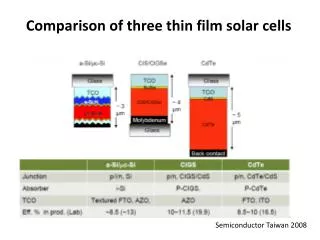
a-Si:H • Record Efficiency : 9.5% (NREL 4/03) • Advantages : • Simple Single Element • Properties are well known • Processes are well estabilished • Disadvantages : • Light-induced Degradation • Low Absorption • Low Exciton Mobility • CdTe • Record Efficiency : 16.5% (NREL 9/01) • Advantages : • Tolerant to deposition methods • Ideal Bandgap • High Absorption and High Efficiency • High stability • Disadvantages : • Strong Fluctuations in Parameters • Difficult to form highly stable ohmic contacts • Difficult to be p-doped • Hazardous Cadmium Contents • CIGS • Record Efficiency : 19.2% (NREL 1/08) • Advantages : • High Absorption and High Efficiency • High Stability • Disadvantages : • Complex Compound • Use of Rare Metals (In,Ga) • Cadmium Contents in Buffer Layer
Structure of CIGS Solar Cell • Substrate Configuration • Well-Studied • 17-19% efficiency • Need Encapsulation • Superstrate Configuration • Lower Cost • Easier Encapsulation • 11-13% efficiency
Front Contact • Development : • CdS:Al → ZnCdS → ZnO/ZnO:Al • (Optical transmittance is increased) • Role of i-ZnO : • Prevent direct contact of CIGS and ZnO:Al • Increase VOC at optimum thickness • ※ TCO deposition temperature should be low • (<150℃)
Role of i-ZnO ZnO:Al CdS CIGS Discontinuity in Conduction Band : ΔEC = χB – χE Discontinuity in Conduction Band : ΔEg = ΔEC + ΔEV
Buffer Layer • n-type semiconductor (bandgap: 2.0~3.6 eV) • PVD-grown CdS show non-uniform coverage • CBD-grown CdS is commonly used • Role of CdS layer : • Optimize band alignment • Mechanical protect against ZnO sputtering • Cd-free Alternatives : • CBD-ZnS (18.1%) • MOCVD-ZnSe • ALD-ZnSe • CBD-ZnSe • PVD-ZnIn2Se4 • Co-Sputtered Zn1-xMgxO • ALD-In2S3
Back Contact • Only Au and Ni ensure ohmic contact • Ohmic behavior at CIGS/Mo interface : • MoSe2 (1.41eV bandgap) formation over 500℃ • Na impurities can aid formation of MoSe2
Absorber • Slightly Cu-deficient composition : • p-type conductivity • High-efficiency with bandgap range 1.2-1.25 eV • [Ga]/[In+Ga] ratio = 25~30%
Composition of Cu-based Chalcopyrites Se In Ga S
Composition of Cu-based Chalcopyrites • Slightly Cu-deficient composition • More Cu-deficient surface layer : stable ordered vacancy compound • Cu(In,Ga)3Se5 • Weak n-type behavior of OVC surface layer • Forming buried pn-junction → minimizes recombination • Formation energies of defects in CuInSe2 are low • Cu vacancy is most favored point defect → Shallow acceptor • 2 VCu + InCu is most favored defect complex → Neutral • 2 VCu + GaCu is less stable • → Hard to form OVC layer • CuInS2 → Hard to form appropriate composition(easy to form CuIn5S8)
Absorber Deposition Methods Ideal CIGS layer : Adequate composition (220/204) orientation Large Grain Conductive CuSe2 phase formation must be prevented
Absorber Deposition Methods - Vacuum • 1. Co-evaporation (19.9%) • Composition can be adjusted by deposition step • OVC layer is formed well • Well-established process • 2. Selenization of Metallic Precursor (14.7%) • Metallic precursor(Cu,In,Ga) deposited by sputtering • Followed by annealing in selenium atmosphere • H2Se is efficient but toxic • 3. Compound-evaporation (9.6%) • Simple and easy to control compared to co-evaporation • lower efficiency • 4. Chemical vapor deposition (No Record) • 5. Close-spaced vapor transport (No Record)
Absorber Deposition Methods – Non-Vacuum • 1. Spray Pyrolysis (4-5%) • Precursors – CuCl2, InCl3, GaCl3, N,N-dimethylselenourea • Impurity(O,C,Cl) incorporation • 2. Electrodeposition (7%) • 15.4% efficiency after PVD stoichiometry correction • 3. Electroless deposition • 13.4% efficiency after PVD stoichiometry correction • 4. Chemical bath deposition • 7.3% efficiency after PVD stoichiometry correction • 5. Chalcogenization of particulate precursor layer (13%) • Precursors – Metallic powder of oxide • Easy to control composition • Toxic H2Se have to be used
Future Works • Atomic pressure plasma treatment on screen-printed CIGS layer • Increase grain size • Adjust Surface and bulk Composition