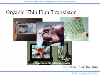
Organic Thin Film Transistor
1.67k likes | 4.76k Vues
Organic Thin Film Transistor. Edited by Song Ho, Kim. Contents. 1. What is the OTFT? 2. Structure of OTFT Application of OTFT Mechanism Operation 5. Pentacene TFT - Proposed Research - Fabrication of Pentacene TFT Characteristics & Analysis

Organic Thin Film Transistor
E N D
Presentation Transcript
Organic Thin Film Transistor Edited by Song Ho, Kim
Contents • 1. What is the OTFT? • 2. Structure of OTFT • Application of OTFT • Mechanism Operation • 5. Pentacene TFT • - Proposed Research • - Fabrication of Pentacene TFT • Characteristics & Analysis • 6. OTFT Materials
What is the OTFT(organic thin-film transistor)? • First Organic Transistor - 1986 • Using organic molecules (Polymers) rather than silicon for their active material. • Semiconductor • Advantages • Less Complex & Lower-cost Fabrication • Solution Processing Photolithographic patterning • lower temperature manufacturing (60-120° C) • Print-able Organic Transistors • Mechanical flexibility • compatibility with plastic substances: foldable & light weight • Strong Optical Absorption and Efficient Emission
Structure of OTFT (2) Various Structures of Organic Thin-Film Transistor Drain Source Semiconductor Dielectric Gate/Substrate Bottom-Contact Top-Contact Top-Gate Bottom-Gate
Structure of OTFT (3) • Differences • Carrier Transport • Discrete Energy Levels • Hopping • Organic Active Layer • Depletion Devices • Very Similar to MOSFETs • 3-Terminal Device • Voltage Controled Switch
Application of Organic TFT (1) OLED Device OLED Display Liquid Crystal Device Plastic TFT LCD Organic Thin Film Transistor E-paper, E-book E-ink Contactless Smart Card Antenna Materials Integration Technology Wearable Computer
Flexible OLED E-paper OLED Technology E-Paper Technology LCD Technology Flexible LCD IC Technology Smart Card RFID Tag Optical Technology Memory device Technology OTFT Sensor Technology Bio Technology Apparel Technology Organic Laser Organic Memory Image Sensor Bio Sensor Electrical Fabric Application of Organic TFT (2)
_ _ source drain pentacene gate dielectric gate glass substrate Mechanism of Operation bias on gate negative positive hole accumulation in pentacene depletion hole flows to drain
Pentacene TFT • substrate - corning7059 glass • gate metal - Nickel • gate dielectric - SiO2 • source/drain metal - Palladium All deposition was performed by Ion beam sputtering Penn. state Univ.
Proposed Research 1. Fabricate Pentacene TFT - gate insulating layer with high dielectric constant - reproducible patterning of pentacene film - source/drain metal with large work function - arrays of pentacene TFT 2. Measurement & Analysis - Vg- Id curve - mobility, threshold voltage, subthreshold slope 3. Evaluation
passivation layer gate dielectric gate source substrate Schematic Figure of Pentacene TFT • substrate - glass (Corning 7059) • gate metal - Al, Ni, Cr • gate dielectric - SiO2, V2O5, Al2O3 • source/drain metal - Au • active layer - pentacene • passivation layer pentacene active layer drain drain
Process Factors • Interfacial effect of metal/gate dielectric - contact resistance, diffusion, dielectric properties • Adhesion of material - film lifting, process unstableness • Making smooth film - the small surface roughness leads to molecular ordering • Photolithographic condition for pentacene patterning - thickness of resist, expose time, develop time - resist/pentacene interface effect
Fabrication Flow Chart Gate sputter, evaporation wet etching Gate dielectric sputter dry etching (RIE) Source/drain sputter, evaporation wet etching, lift-off Pentacene ICBD, evaporation wet & dry etching Passivation CVD dry etching (RIE)
Gate Dielectric Layer Requirement • fabricated at low temperature ( < 300°C) • smooth surface roughness • have a high capacitance with low leakage current • good phase stability • reproducibility SiO2, V2O5, Al2O3
Analysis of Gate Dielectric Layer C-V Electrical characteristics I-V Deposition by Reactive sputtering AFM Roughness I-V Au deposition on gate dielectric and annealing Interfacial effect RBS
-6 1.0x10 -7 8.0x10 ) 2 -7 6.0x10 F/cm -7 4.0x10 R.T 200µµ 2hr -7 2.0x10 Capacitance ( 200µµ 3hr 300µµ 0.0 400µµ SiO -5 0 5 10 15 2 Voltage (V) C-V Analysis of V2O5 Dielectric Material
Deposition of Pentacene Film Deposition technique • Evaporation • ICBD (Ion Cluster Beam Deposition) expected to evaluate pentacene properties Simple structure estimate pentacene properties
Patterning of Pentacene Film Photolithographical method - using photosensitized PVA as negative photoresist - UV expose & develop in water - etching unwanted pentacene layer in oxygen plasma - baking to remove water in pentacene layer photosensitized PVA pentacene dielectric layer
Operation Characteristics • Field effect mobility(fe ) and the threshold voltage(Vth) were obtained in the saturation region using the relation • Positive threshold voltage arise from an initial accumulation layer at the pentacene/dielectric interface - positive gate voltage is required to turn the device fully-off • Large on/off current ratio can be obtained with small gate voltage swing
Different Structure of Pentacene TFT pentacene active layer • 3 mask steps • no overlap gate-source, gate-drain gate dielectric gate source drain substrate • pentacene layer is normally conducting no overlap gate-source, gate-drain large drain current to flow at zero gate bias devices are turned off by applying positive gate bias transistor operating in depletion mode
Number Name 133 • PentaceneBenzo[b]naphthacene • 2,3:6,7-Dibenzanthracene • beta,beta'-Dibenzanthracene • 2,3,6,7-Dibenzoanthracene • lin-Dinaphthanthracene • lin-Naphthanthrene CAS: 135-48-8 M W: 278 L / B: 2.226 Width: 7.447 Length: 16.577 Thickness: 3.885 Structure of Pentacene
p-Type Materials Structure and mobility of fused aromatic Compounds
p-Type Materials Oligo-thiophenes and Oligo-phenylenes
p-Type Materials Thiophenylenes and their mobilities
p-Type Materials Conjugated polymers for FET Polythiophene materials for FET
Hall Mobility Change of Polythiophenes Hall mobility change of Poly(2-alkylthiophene)s by arrangement and stereo chemistry
n-Type Materials Quinodimethane compounds Tetracarboxylic anhydrides Phthalocyanines
n-Type Materials Fluorinated n-type materials
Structure of General FET Low Current and low operating speed Low conductivity and low carrier mobility of Organic semi-conductor High purity crystallinity Improvement of physical properties Searching of New materials Improvement of Device Structure SIT New mechanism Phase Transition FET Problem and Solution of OTFT
Reference 1) 고분자 과학과 기술 제 17권 1호 2006년 2월 ‘유기반도체 재료’ 하승규, 권오식 2)고분자 과학과 기술 제 14권 5호 2003년 10월 ‘유기트랜지스터 재료 연구개발 동향’ 권순기,김윤희,김형선,안준환 3) 고분자 과학과 기술 제 15권 6호 2004년 12월 ‘고분자박막트랜지스터 개발동향’ 김보성,이용욱, 홍문표, 정규하 4)화학세계 04/06 50 ‘단분자 OLED재료 및 OTFT 재료의 개발동향’ 권순기 3)고분자 과학과 기술 제 14권 1호 2003년 2월 ‘유기’ 하승규, 권오식 5) University of the South Sewanee, Tennessee September 2002, Eugene Donev ‘Designing and Implementing Organic Thin-Film Transistors (OTFTs)’ 6) Adv. Mater. 2000, 12, No. 7 p.481 , Groenendaal,* Friedrich Jonas, Dieter Freitag, Harald Pielartzik, and John R. Reynolds ‘Poly(3,4-ethylenedioxythiophene) and Its Derivatives: Past, Present, and Future’
Reference 7) Ali Ali Afzali Afzali, Christos Christos D. D. Dimitrakopoulos Dimitrakopoulos IBM Research Division T. J. Watson Research Center T. J. Watson Research Center Yorktown Heights, NY ‘Synthesis and Application of Pentacene Precursor in OTFT’ 8) Chang Feng Yu ,Ching Fu Hsu, Yao Peng Chen, and Yu Hua Ma Department of Information and Communication Engineering Chaoyang University of Technology ‘Dependence of field-effect mobility on the gate field for Pentancene OTFTs’ 9) http://chem3.snu.ac.kr/ ~shlee/OTFT.htm 10) http://www.postech.ac.kr/ ce/lamp/research-4.html 11) http://www.organicid.com/structure.html