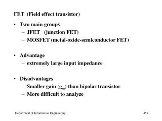
Organic Field Effect Transistor
Organic thin film field-effect transistors (OTFTs) are particularly interesting as their fabrication processes are much less complex compared with conventional Si technology, which involves high-temperature and high-vacuum deposition processes and sophisticated photolithographic patterning methods. In general, low-temperature deposition and solution processing can replace the more complicated processes involved in conventional Si technology. In addition, the mechanical flexibility of organic materials makes them naturally compatible with plastic substrates for lightweight and foldable products. Since the report of the first organic field-effect transistor in 19861, there has been great progress in both the materials' performance and development of new fabrication techniques. OTFTs have already been demonstrated in applications such as electronic paper2, 3, 4, sensors4, 6, and memory devices including radio frequency identification cards (RFIDs)7, 8. Although OTFTs are not meant to replace conventional inorganic TFTs – because of the upper limit of their switching speed – they have great potential for a wide variety of applications, especially for new products that rely on their unique characteristics, such as electronic newspapers, inexpensive smart tags for inventory control, and large-area flexible displays.<br><br>

Organic Field Effect Transistor
E N D
Presentation Transcript
OPTO−ELECTRONICS REVIEW 18(2), 121–136 DOI: 10.2478/s11772−010−0008−9 Organic field-effect transistors M.J. MAŁACHOWSKI1and J. ŻMIJA*2 1Department of Technical Education, Technical University of Radom, 29 Malczewskiego Str., 26−600 Radom, Poland 2Institute of Technical Physics, Military University of Technology, 2 Kaliskiego Str., 00−908 Warsaw, Poland Thepaperreviewstherecentyearpublicationsconcerningorganicfield−effecttransistors(OFETs).Alotofworkshavebeen performed to help understanding the structural and electrical properties of materials used to construct OFETs. It has been established that in partially ordered systems, the charge transport mechanism is thermally activated and field−assisted hopping transport and the hopping transport between disorder−induced localized states dominate over intrinsic polaronic hopping transport seen in organic single crystals. Many research attempts have been carried out on the design of air−stable organic semiconductors with a solution process which is capable of producing OFETs with excellent properties and good stability when subjected to multiple testing cycles and under continuous electrical bias. Recent experiments have demon− strated ambipolar channel conduction and light emission in conjugated polymer FETs. These achievements are the basis for construction of OLED based displays driven by active matrix consisting of OFETs. Keywords: organic electronics, organic field−effect transistors, opto−electronic materials, information displays. 1. Introduction systems and organic field−effect transistors (?FETs) are in active development (in order to indicate the transistor struc− ture, through this paper we shall use also OTFT, OFET or OTFFET abbreviations for organic thin film transistor, however, all transistors considered here operate as the field effect devices). The processing characteristics and demon− strated performance of OFETs suggest that they can replace existing or be useful for novel thin−film−transistor applica− tions requiring large−area coverage, low−temperature pro− cessing, mechanical flexibility and, especially, low cost. Such applications include switching devices for active−ma− trix flat−panel displays (AMFPDs) based on either liquid crystal pixels (AMLCDs) or active matrix with organic light− −emitting diodes (AMOLEDs). At present, hydrogenated amorphous silicon (a−Si:H) is the most commonly used as active layer in TFTs backplanes of AMLCDs. The higher performance of polycrystalline silicon TFTs is usually re− quired for well−performing AMOLEDs. Improvements in the efficiency of both the OLEDs and the OTFTs could broaden applications. OTFTs could also be used in active− −matrix backplanes for “electronic paper” displays based on pixels comprising either electrophoretic ink−containing microcapsules or “twisting balls”. Other applications of OTFTs include low−end smart cards and electronic identifi− cation tags. Most of the investigated OFETs are not all organic as well as not flexible ones. The devices are usually con− structed on no flexible silicon substrate. In order to fabri− cate the flexible AMOLED structure, rather all−organic In the inorganic semiconductors such as Si and Ge, the at− oms are held together with very strong covalent bonds, as high as 300 kJ/mol for Si. In these semiconductors, charge carriers move as highly delocalized plane waves in wide bands and indicate a high mobility of charge carriers μ >> 1 cm2/Vs. In organic semiconductors, intramolecular interac− tions are also mainly covalent, while intermolecular interac− tions are usually induced by much weaker van der Waals and London forces resulting in energies smaller than 40 kJ/mol. Thus, the transport bands in organic crystals are much narrower than those of inorganic ones, and the band structure is easily broken by disorders in such systems, leading to creation of states in the energy gap. Almost all organic solids are insulators. However, in or− ganic crystals that consist of molecules that have the ?−con− jugate system, electrons can move via ?−electron cloud overlaps. That is why these crystals exhibit electrical con− ductivity. Polycyclic hydrocarbons and phthalocyanide salt crystals are examples of this type of organic semiconductor. Among the conjugated polymers there exist conductive and semiconductive polymers. Organic semiconductors, such as conjugated oligomers and polymers, have become materials for a wide range of not only electronic but also optoelectronic devices. Organic light−emitting diodes (OLEDs) inserted into commercial *e−mail: jzmija@wat.edu.pl Opto−Electron. Rev., 18, no. 2, 2010 M.J. Małachowski Unauthenticated Unauthenticated Download Date | 9/24/15 11:36 PM Download Date | 9/24/15 11:36 PM
Organic field−effect transistors FETs should be used. The three−dimension bottom struc− ture of this device is shown in Fig. 1(a). Figures 1(b) and 1(c) present top and bottom structures, respectively, cross sections of not all organic TFTs because heavily doped silicon and metal electrodes are used to fabricate them. Both types of construction were extensively studied and their advantages as well as disadvantages have been shown. The investigation results of various soluble organic se− miconductors show that, ?? ?−dihexylsexithiophene (DH−6T) has become the most promising candidate for all−organic semiconductor integration because of its air stability, good solubility, and easy synthesis. For these purposes, the polymethylmethacrylate (PMMA) is used as a dielectric layer to substitute SiO2in order to confer the transfer characteristics of OTFTs with PMMA as a dielectric layer. All−organic TFTs on flexible polyimide substrates can be produced indicating electricalperformance similarto that of TFTs fabricated with inorganic gate dielectrics and metal contacts. For production the OFET devices, a technique can be based on area−selective electropolymerization on a pre− patterned anode. Source and drain contacts can be poly− meric. The active semiconducting layer can be deposited by spin coating of an appropriate solution. The gate dielectric layer can be prepared by spin coating a solution of insulat− ing polymer. The aim of numerous studies on OTFTs of configurations shown in Fig. 1 or similar are to improve the transistor performance, which includes almost all elements of the device as well as the charge transport mechanism between source and drain. Progress in plastic electronics is achieved mainly by rising in the mobilities of organic semiconductors, increase in the capacitance of suitable gate dielectrics, and reduc− tions in the channel dimensions of the devices. Both poly− mer and small molecule−based organic thin films may be used in OFET technology. Mobile charge carriers of either polarity can be injected into organic semiconductors from contacts of suitable materials. The mobilities of these charge carriers, however, are low in comparison to inor− ganic semiconductors, and the device performance is often strongly lowered by carrier trapping. The transport mecha− nism is best described as a hopping process and the charge carriers are polarons. For brevity, a conventional semicon− ductor language is used to refer to the negative charge carriers as electrons and to the positive charge carriers as holes. The purpose of this article is to review the recent most important papers concerning the investigations on the ef− fects governing the operation of OFETs, which have a thin film as well as crystalline form. There are known some reviews focused at different problems connected with OFETs, just to mention the papers [1–6] and others [7,8]. 2. Charge transport in organic semiconductors and OFETs As it was mentioned above, organic semiconductors have major drawbacks in relatively low mobility of charge car− riers arising from weak intermolecular interaction in solid state and in the fact that doping is problematic because it is interstitial and not substitutional as in inorganic semi− conductors. An organic semiconductor is considered with the VBor the highest occupied molecular orbital (HOMO) and the CBor the lowest unoccupied molecular orbital (LUMO) which are separated from each other by the gap which is usually rather large, EG> 2 eV. For organic semiconductors, the manifolds of both the LUMOs and the HOMOs are characterized by random positional and energetic disorder. To model the current flow in organic semiconductors, the charge transfer complex (CT complex) idea is intro− duced. CT complex is defined as a pair of molecular groups, where one is electron−donating (donor) and the other is elec− tron−accepting (acceptor) and where there is a partial trans− fer of charge from the acceptor to the donor in an excited molecular state. CT complexes have a transition between Fig. 1. Three−dimensional view of an all−organic bottom structure thin film field effect transistor (a), top electrode structure of OTFT (b), and bottom electrode structure of OTFT (c). 122 Opto−Electron. Rev., 18, no. 2, 2010 © 2010 SEP, Warsaw Unauthenticated Unauthenticated Download Date | 9/24/15 11:36 PM Download Date | 9/24/15 11:36 PM
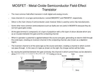
3. Principles of operation of MOSFETs and TFFETs the excited molecular state and a ground state and almost all CT complexes have absorption bands in the ultraviolet or visible region. The interaction between donor and acceptor is not only a charge transfer interaction but also electrostatic force. This kind of interaction is usually much weaker than interactions of the hydrogen bond and the covalent bond, but it is essential for constructing the crystal structures. Since the HOMO level in most organic semiconductors is deep, the gap separating LUMO and HOMO states, as men− tioned above, is wide, energies of donor and acceptor mo− lecules are normally well below LUMO and above HOMO levels. In 1962, an important acceptor, tetracyanoquinodimetha− ne (TCNQ), was exploited and in 1970, an important donor, tetrathiafulvalene (TTF), was synthesized. In 1973, a CT complex composed of the TTF and TCNQ was discovered, it was the organic conductor. In a crystal of TTF−TCNQ, the TTF and TCNQ are stacked independently and an electron transfer from donor (TTF) to acceptor (TCNQ) occurs. Hence, electrons and holes can transfer in the TCNQ and TTF columns, respectively. It is possible to interfere in the columns ordering. A well known theory by Mott [9] assumes that the con− duction process in organic materials is entirely determined by the tunnelling transitions of carriers between localized states, provided that the electronic wave functions of the lo− calized states have sufficient overlap. The transport proper− ties of many organic semiconductors can be well described by the variable range hopping theory VRH [10,11]. Despite decades of researching progress, however, there are still some effects of the charge transport in organic semi− conductors to be explained. An interesting approach in the understanding of the transport of charge carriers in organic semiconductors has been elaborated in the theoretical and experimental study by Li et al. [12]. In that work, it is presented an ana− lytical model for hopping transport in doped, disordered organic semiconductors based on the VRH and the perco− lation theory. It was assumed in Ref. 12 that localized states are randomly distributed in both the energy and the coordinate space, and that they form a discrete array of sites. Conduction proceeds via hopping between these sites. The mobile carrier density and its mobility are the main parameters determining the charge transport in organic semiconductors. The mobile electron and hole densities in a semiconductor, inorganic or organic one, are in any case determined by the distribution of transport states, which is characterized by their density of states (DOS). For thermo− dynamic equilibrium it is not of interest whether the states are extended or localized and whether one has correspond− ingly band conduction or hopping conduction. In the case of a conjugated polymer, where the carriers are polarons, one has to consider just these polaron states. In any case, the dis− tribution of the transport states is characterized by their DOS. 3.1. Silicon single crystal MOSFET We shortly discuss some well understood principal effects oc− curring in commonly used silicon single crystal (metal oxide semiconductor field effect transistors – MOSFETs). A MOSFET structure consists of a p−type silicon single crystal semiconductor on which two n+electrodes have been formed creating the source and the drain contacts. The third electrode, the gate, which is used to modulate the conductivity of the source−drain channel, is isolated from the semiconductor sub− strate by an insulating (oxide) layer. A depletion region in which the concentration of charge carriers is lower than in the bulk is generated near the source and the drain electrodes. This kind of transistor appears to be most often used in the elec− tronic circuits, however, there are another transistor structures differing from MOSFET device. When a sufficiently high positive voltage is applied to the gate of a MOSFET, an inversion layer forms interface between the insulator and semiconductor, providing a con− ducting channel between the source and the drain. This turns the device on. One of main advantages of the MOSFET structure is that the depletion region between the p−type substrate and both the n−channel and the n+regions below the source and drain contacts provides isolation from any other device fabricated on the same substrate. Very low off currents are also achieved because the both n+regions act as reverse−biased diodes. If we assume that the channel length L is much larger than the insulator thickness t and that the charge mobility ? is constant, the drain current IDis related to the source−drain voltage VDand the source−gate voltage VGin the folowing way W C ? ? ? ? ? ?? ? ?? V i D 2 ? ? ? ? 2 I V V D G B D L (1) ? ?? ?? ? ? ? 2 qN 2 3 S A 32 32 ? ? ? ? ?B V ( 2 ) ( 2 ) D B C i where W is the channel width, Ciis the insulator capacitance (per unit area), ?sis the semiconductor permittivity, and NA is the doping level of the p−type substrate. Equation (1) pre− dicts that, for a given gate voltage, the drain current first in− creases linearly with the drain voltage (linear regime), then gradually levels off to a constant value (saturation regime). It also predicts that the drain current increases when the gate voltage increases. For a small VD, Eq. (1) is reduced to Eq. (2), where VTis the threshold voltage, which corresponds to the onset of the strong inversion regime, is given by Eq. (3) W C ? i ? ? , (2) V ( V ) I V D G T D L ? ? 4 qN S B A ? ? ? where . (3) 2 V T B C i 123 Opto−Electron. Rev., 18, no. 2, 2010 M.J. Małachowski Unauthenticated Unauthenticated Download Date | 9/24/15 11:36 PM Download Date | 9/24/15 11:36 PM
Organic field−effect transistors Two important technological parameters are the channel conductance gDand the transconductance gm, which, in the linear regime, are given by Eqs. (4) and (5), respectively. In the saturation regime, the drain current and transconduc− tance are given by Eqs. (6) and (7), respectively ration may compete or totally replace the previous one if the molecular material is deposited onto a thin dielectric layer covering a conductive gate. By applying a potential between the source and the gate, charges are created on the two sides of the insulating layer following the equation W C ? ? ? I V Q = CV, i D ? ? ? ) , (4) V ( g V D G T L where Q is the electric charge, C is the capacitance, and V is the voltage. The drain−to−source current can therefore be modulated by the gate−to−source voltage. At sufficiently high VDSvoltages, injection of charge carriers from the elec− trodes is possible. The probability of electron transfer from (or to) the electrode to (or from) the molecular material de− pends on the energy difference between the Fermi level of the metal and the HOMO and LUMO levels. The results described so far demonstrate that the mole− cular material based field effect transistors are original from a fundamental point of view, they differ totally from sili− con−based devices for both the charge transport mechanisms (hopping model against band theory) and physicochemical reasons which afford the modulation of the drain−to−source current by a gate voltage. The molecular FET may show fairly good mobilities, high ION/IOFFratios and respectable stabilities in air. When rapid switching times are not re− quired, the molecular FET could be used in practical appli− cations. For this reason, care has to be taken when transfer− ring the equations of the drain current from the MOSFET to the TFFET. The absence of a depletion region leads to a simplification of Eq. (1), which can now be written as DV ? const G W C V ? ? ? I V i D D ? ? , (5) g m L GV ? const D W C ? 2 i 2, ? ? (6) V ( ) I V D sat , G T L W C ? i ? ? ). (7) V ( g V m G T L 3.2. Thin film transistor In order to apply the accumulation effect in the structure of thin film field effect transistors (TFFETs), the low conduc− tivity materials are used and amorphous silicon layer is an example of such a material. This remark can be adapted, in most cases, for the organic materials. However, it should be mentioned that the attempts have been made to achieve the field effect transistor behaviour in inorganic semiconduc− tors of moderate conductivity [13]. To achieve this, a very thin filmof active materialshould be used to develop the de− pletion region. The above described type of a process taking place in MOSFETs, does not occur for organic materials which are insulators (rather than semiconductors) when undoped (with the exceptions of Pc2Lu and PcLi). In most conductivity measurements of organic materials, the inten− sities of current measured are, in most cases, very small. The use of field effect could permit us to alleviate this diffi− culty. To achieve this effect, an electron−active molecular material thin film is deposited on a dielectric (SiO2, Si3N4, polymers) of very small thickness (100–200 nm) covering a metallic electrode (the gate). Two gold electrodes (source and drain) separated by the distance L are then deposited on the molecular material. The source and drain electrodes form ohmic contacts di− rectly to the conducting channel. Unlike the MOSFET structures described above, there is no depletion region to isolate the device from the substrate. Low off currents are only guaranteed by the low conductivity of the semi− conductor. A second crucial difference to the MOSFET is that, the OFET operates in the accumulation regime and not in the inversion regime. Let us consider that the molecular mate− rial does not possess a significant density of intrinsic charge carriers. When a drain−to−source voltage is applied, no cur− rent (or a negligible one) can flow from one electrode to the other. The molecular material behaves as an insulator if the quantity of charges injected from the electrodes (injected current) is small. Another mechanism of charge carrier gene− W C ? ? ?? ? ?? V i D 2 ? ? ? . (8) I V V V D G T D L Here, the threshold voltage is the gate voltage for which the channel conductance (at low drain voltages) is equal to that of the whole semiconducting layer. It is given by Eq. (9), where N is the density of doping centres (donors or ac− ceptors, depending on whether the semiconductor is n or p−type) and d is the layer thickness. Equation (9) assumes that all doping centres are ionized, which is far from being the case in organic semiconductors, as will be seen later. qNd C ? . (9) V T i In the saturation regime, the current is given by Eq. (6). We must be aware that this equation was derived under as− sumptions that are not always fulfilled in organic semicon− ductors, particularly that of a constant mobility. The current characteristics of OTFTS often show a dis− advantageous nonlinearity at low drain voltages. In topcon− tact OTFTs this effect can be caused by trap recharging if the contacts are of Schottky type. For bottom contact OTFTs, Schottky contacts as origin of the nonlinearity are often stated. A Schottky contact only at drain leads to such a nonlinearity. However, with the same Schottky contacts at drain and source, the effect is covered by the high resistance of the contact at a source. Further, it was demonstrated with 124 Opto−Electron. Rev., 18, no. 2, 2010 © 2010 SEP, Warsaw Unauthenticated Unauthenticated Download Date | 9/24/15 11:36 PM Download Date | 9/24/15 11:36 PM
and ? + Egfor holes where ? is the electron affinity acts as barrier at the contacts. Since the p−type organic layers are most common, such electrodes as ITO or CuxSe as the hole carrier sources should be more intensively studied. The structure of energy level scheme is shown in Fig. 3 (after Refs. 16 and 17) for a p−doped semiconductor. The contact formation leads to a common Fermi level. The ener− gy zero is chosen at the Fermi level ?F. The contact forma− tion is connected with the position dependent potential ener− gy V(x) which approaches in the bulk semiconductor the bulk intrinsic energy level which is denoted by Vbulk. The to− tal drop in V(x) has to compensate the built−in potential Vbi, i.e., the work function difference between the semi− conductor and the metal. simulations [14] that the combination of the presence of Schottky contacts with a field dependence of the mobility can cause the nonlinearity. 4. Examples of energy bands in organic semiconductor devices The shape of the energy bands appearing in organic semi− conductor devices, especially at the contact area, is essential in understanding the transport processes in a particular de− vice. Almost all OFETs have the structure with low work− −function electron and high work−function hole injecting source/drain contacts to a conjugated polymer organic semi− conductor. On the basis of Ref. 15 we show the energy band shape through a channel. It was considered the source−semi− conductor−drain structure in the form of metal−pentacen− −P13−metal (Fig. 2). Here, source and drain are made from two different metals (Au and Mg), and as a consequence of the unequal metals for source and drain contacts and the layer arrangement, two cases have to be discussed in which either Au or Mg is used as source contact. The corresponding band scheme is depicted in Fig. 2. The bilayer is formed from pentacene as electron−transport material and NN −ditridecylperylene−3, 4, 9, 10−tetracar− boxylic diimide (P13), as hole transport material. The two different contact metals for source and drain, respectively, were chosen to provide efficient electron and hole injection. SiO2serves as gate insulator. The work functions of the me− tallic source and drain contacts are crucial quantities and should be chosen individually to enable efficient injection of holes from one and electrons from the other contact. Thus, for the Au contact it was chosen Au = 5.0 eV, which is close to the valence band (highest occupied molecular or− bital – HOMO) of pentacene (Fig. 2). The work function for the Mg contact ?Mghas been varied; 3.635 or 3.66 eV is used. The difference between these metal work functions and the energy of the transport states; i.e., ? for electrons Fig. 3. Energy scheme of a contact between metal (left) and semi− conductorlayerofthethicknessd(right), with valenceandconduc− tion band edges, or centers of the HOMO and the LUMO distribu− tions ?vand ?cwith the common Fermi energy ?F. The position de− pendent potential energy V(x) and the built−in potential Vbi(after Ref. 17). 5. Charge transport along an OTFT channel Charge injection phenomena and the impact of source and drain contact resistances have been established to play a cru− cial role in the OTFTs performance. The physics of these ef− fects is still a subject of active investigation. In OTFTs a low conductivity in the bulk layeris required fora large on−offcur− rent ratio. When the bulk conductivity is not negligible, there appears crossover effect from field−effect dominated current to the bulk dominated current in the transfer characteristics of a doped accumulation mode disordered organic transistor. Conventionaldeviceswithanunshieldeddrainelectrodesuffer from parasitic currents outside the channel area, which may obscure the crossover from field−effect dominated current to bulk dominated current. Fig. 2. Band scheme for the structure of metal−pentacen−P13−metal transistor along the channel (x axis) and perpendicular (y axis) to− ward the Mg top contact. Affinities, gaps and work functions are given in eV. Correspondingly, the hole (electron) injection barrier (boldlines)attheAu(Mg)contactis0.07eV(0.26eV),andtheelec− tron barrier from P13 to pentacene (hole barrier from pentacene to P13) is 0.18 eV (0.33 eV) (after Ref. 15). 5.1. p-type channel OFETs Most of the OFETs that have been described to date have a p−type channel. A typical output characteristic of the pen− tacene based on the thin film OFET is shown in Fig. 4 [18]. 125 Opto−Electron. Rev., 18, no. 2, 2010 M.J. Małachowski Unauthenticated Unauthenticated Download Date | 9/24/15 11:36 PM Download Date | 9/24/15 11:36 PM
Organic field−effect transistors −work function metals as source−drain electrodes exhibit n−type characteristics under oxygen−free conditions [21,22]. Recently, Chua et al. [23] stated that the trapping of elec− trons by the hydroxyl groups on the surface of SiO2gate di− electric layer affected the n−channel conduction of OFETs. Most conjugated polymers yield n−type characteristics when a suitable hydroxyl−free polymer, such as a divinyltetra− methylsiloxane− bis(benzocyclobutene) derivative, is used as the gate dielectric. Accordingly, the properties of the in− terface between the gate dielectric and the organic active layer are critical to the transport and accumulation of posi− tive or negative type of charge carriers. Pentacene is fre− quently used as an active layer for p−type OFETs, but it was found that it exhibits the n−type characteristics as well [24,25]. The n−type transport in OFETs incorporating pentacene on a SiO2dielectric has been demonstrated [17]. The beneficial effect ofa thin layer of oxidized Ca between the SiO2dielectric and pentacene on the electron transport properties in OFETs has been analyzed in detail [23]. The poly(4−vinyl phenol) (PVP) polymer layer is a hydroxyl− −group−rich polymer dielectric, which is considered to inter− fere with the conduction of electrons for n−type OFETs, as proposed by Chua et al. [23]. Presumably, the hydroxyl or the polar groups on the PVA dielectric favour the formation of n−channel conduction in the pentacene active layer, and these groups have different functionalities from those on the SiO2gate dielectric. Typical IDSvs VDScharacteristics in the case of n−type channel pentacene−based OFET fabricated on the PVA cross−linked PVP dielectric, operated at a positive VG, are shown in Fig. 5 [26]. Fig. 4. Output characteristics of polymer film formed on SiO2gate insulating layer treated with OTS (after Ref. 16) immersed in a 50−mM solution of a fresh organosilane, octyltrichlorosilane (OTS). The characteristic is typical for transistors having the p−type accumulation channel. The studies of Wang et al. [19] gave us progress in un− derstanding of the charge transport mechanisms in the chan− nel of polycrystalline organic semiconductors. The group has fabricated OTFTs, using pentacene as the active layer. Experimental data suggested that thermally activated and field−assisted hopping transport between disorder−induced localized states, dominates the intrinsic polaronic transport seen in organic single crystals. The experimental results have been found to exhibit a Frenkel−Poole−type depend− ence consistently over a wide range of channel lengths, fields, and temperatures. Hamadani et al. [18,20] have reported the results of in− teresting investigation of a field dependence of the longitu− dinal mobility in OFETs based on poly(2,5−bis)3−tetra− decylthiophene−2−yl(thieno)3,2−b(thiophene) (pBTTT−C14) as the active polymer layer. Devices were fabricated in a bottom−contact configuration on a degenerately doped n+ silicon wafer as a gate. The gate dielectric is 200 nm of ther− mally grown SiO2. The electrodes are deposited by thermal evaporation of Ti and Au. The devices operated as standard p−type OFETs in accumulation mode, the output charac− teristics are shown in Fig. 4. 6. Gate insulators for OTFTs A remarkable amount of papers have been devoted to study different dielectric materials that can play the role of the gate insulators in OTFTs. In addition to the conventional in− 5.2. n-channel OFETs As mentioned above, most papers that have appeared to date are devoted to the p−type channel OFETs but few have an n−type channel, Ref. 20 is an example. OFETs with high− −electron−affinity organic materials as active layers or low− Fig. 5. IDSvs. VDSplots of pentacene−based OFET fabricated on PVA/cross−linkedPVPdielectric,operatedatthepositiveVGinthe n−channel conduction regime (after Ref. 26). 126 Opto−Electron. Rev., 18, no. 2, 2010 © 2010 SEP, Warsaw Unauthenticated Unauthenticated Download Date | 9/24/15 11:36 PM Download Date | 9/24/15 11:36 PM
organic materialssuchas SiO2, Al2O3, and HfO2, various or− ganic materials were also tried for the gate dielectric in OTFTs. Insulating polymers including poly−4−vinylphenol, polymide, parylene, and polyaniline have been successfully employed for the gate dielectric and haveshown to enhance device performance. In addition, polymethyl methacrylate (PMMA) derivative polymers are one of the new materials for the gate dielectric or buffer layer, exhibiting high field− −effect mobility and low threshold voltages. A wide used SiO2dielectric as a gate insulator can play a different role in OFETs depending on its surface treating, even change in the channel type can be achieved. Mis− kiewicz et al. have demonstrated that the surface energy of the dielectric can have large impact on the performance of FETs based on TTF−4SC18 [27]. Average charge carrier mobility was 30 times increased as a result of proper treat− ing. The surface energy of the employed SiO2dielectric de− creased. The authors pointed out that the performance of the OFETs produced on SiO2depends also on such factors as surface energy and method of organic semiconductor depo− sition, in addition to the surface roughness. The achieved μFETof 0.2 cm2/Vs is among the best results published for large area solution−processed OFETs prepared and mea− sured in air, especially taking into account the reprodu− cibility and uniformity of zone−cast layers. 6.1. Influence of higher dielectric constant Some studies are devoted to obtain the gate insulator of high dielectric constant and strength and proper interaction with the active semiconductor leading to improvements in OFET performance. SiO2film appears to be a good insulator and has a very high dielectric strength, approximately 10 MV/cm. However, the dielectricconstant of SiO2is not very high, approximately ? = 4. Thus, many research groups have been trying to fabricate OFETs on a high dielectric constant gate insulator to inject more carriers. Another advantage of high−? materials is a lower operating voltage. There has been shown very clearly the beneficial role that plays the high dielectric constant tantalium oxide (Ta2O5) as a gate insulator [28,29] in OFETs. In order to improve the carrier injection, Ueno et al. [29] have studied carrier injection into OFETs with Ta2O5as a gate insulator. Figure 6(a)shows the drain current vs. drain voltage characteristics of a p−type pentacene OFET as a function of the gate voltage. As shown in Fig. 6(b), this OFET operated also at low gate/drain voltages due to the high dielectric constant of the Ta2O5gate material. For the p−type OFET, the reverse negative bias voltage was applied between the gate and source electrodes, corre− sponding to the reverse voltage to the anodized Ta2O5/Ta gate. The investigation result shows that the anodized Ta2O5/Ta gate can also work as the gate capacitor for an n−type OFET. It has been shown that using high−? gate structure provides possibility of injection a higher amount of charge carriers into organic active layers than on the SiO2/Si gate conventionally used in most OFETs. Fig. 6. Drain current vs. drain voltage characteristics of a p−type pentacene OFET fabricated on the Ta2O5/Ta gate as a function of gatevoltage(afterRef.29):(a)highvoltageand(b)lowvoltageop− erations. 6.2. Gate dielectrics on flexible substrates It should be also indicated that the SiO2film is grown onto unflexible silicon substrate. The organic gate dielectric is a key ingredient for the realization of all−organictransistors, which is important for flexible display and other low−cost device applications. As an example, in order to make possi− ble application of OFETs on flexible substrates, Parashkov et al. [30] have fabricated fully patterned all−organic TFTs with a variety of organic polymer insulators and the gates printed on top of the gate dielectric layer. The group has produced OTFTs on flexible polyimide substrates and ob− tained devices with electrical performance similar to that of OTFTs fabricated with inorganic gate dielectrics and metal contacts. Majewski et al. [31] have investigated bottom−gate OFETs using a commercially metallized Mylar films coated with an ultra−thin (3.5 nm) SiO2layer as a flexible substrate. The OFETs have been fabricated using this substrate, regio− regular poly(3−hexylthiophene) (rr−P3HT) as a p−type semi− conductor, and gold source and drain contacts. This resulted in OFETs that operated with voltages of the order of 1 V. 127 Opto−Electron. Rev., 18, no. 2, 2010 M.J. Małachowski Unauthenticated Unauthenticated Download Date | 9/24/15 11:36 PM Download Date | 9/24/15 11:36 PM
Organic field−effect transistors 7. Doping The doping process of organic semiconductors can largely be depicted by a standard model used for crystalline inor− ganic semiconductors, a general doping model still remains a challenge for organic semiconductors. In particular, for some experiments, a strong superlinear increase in the con− ductivity with doping is observed. One of the limiting mechanisms in OFETs performance is an increase in p−type doping due to a charge−transfer reac− tion with ambient atmosphere. An increase in doping leads to an increase in the conductivity of the bulk semiconductor, which reduces the current modulation, or on−off ratio, of the transistor. The polymers P3HT and PTV, exhibit a dopant density increase upon air exposure in the dark, which re− quires a reevaluation of the doping mechanism in terms of a charge−transferreaction with oxygen under light exposure. Chen et al. [32] have studied the impact of FeCl3doping on polymer−based TFTs (PTFTs) performance. It has been ob− served that field effect mobility of rr−P3HT can be increased by two orders of magnitude from 7.2×10⁻⁴cm2/Vs to 7.4×10⁻²cm2/Vs by doping with FeCl3. The results suggest that FeCl3doping may induce changes in the interface states between P3HT and Au. Since the interface states may vary from material to material, dopants other than FeCl3may be needed to reduce the contact resistance with Au electrode. Interesting results have been reported by Li et al. [12]. Their experimental and theoretical studies indicated that conductivity of the organic semiconductors strongly de− pends on doping and temperature. The temperature depend− ence of the carrier conductivity for different doping concen− trations the research group illustrated experimentally in the graphical form. The Arrhenius−type temperature depen− dence ? ? Fig. 7. Temperature dependence of conductivity in a disordered hopping system at different doping concentrations (after Ref. 12). Figure 7 illustrates the temperature dependence of the conductivity for different doping concentrations [12]. The Arrhenius−type temperature dependence, Eq. (10), can be observed clearly in Fig. 7. It was concluded that at higher temperatures, almost all the carriers occupy the intrinsic states, therefore the dopants do not change the trap−freehop− ping process. The doping process is quite efficient for ZnPc with dopant F4−TCNQ. 8. Traps Organic semiconductors often contain significant densities of charge carrier traps, and carrier trapping at the organic semiconductor/gate insulator interface can be important in OFETs operation. The importance of trapping decreases with increasing charge carrier densities because traps are filled and thus become inactive. When the carrier densities are small the devices are particularly sensitive to carrier trapping. Some of the injected electrons and holes occupy localized trap states and are not mobile. This effect is mo− delled by treating the carrier mobilities as density depen− dent, with low carrier densities implying low mobilities. Goldmann et al. [35] have investigated charge trapping in rubrene single−crystal OFETs with two different typical and frequently employed interfaces, an untreated SiO2di− electric/semiconductor interface and a chemically treated SiO2/semiconductor interface. A reversible and reproduc− ible shift of the I−V characteristics is observed upon both negative and positive gate bias stress. The physical origin of these results is identified as charge trapping and detrapping at the crystal/SiO2insulator interface on a time scale of 1 h. Figure 8 presents energy distribution of the DOS at an organic single−crystal/dielectric interface [35]. Etdenotes the demarcation energy between the occupied and the unoccupied traps. Part of the unoccupied traps be− tween EFand Etwill capture the charge carriers relatively quickly, i.e., on a time comparable to the OFET measure− ment time 10 s to 1 min, and will appear as hysteresis in the ? ? ? k T B E A ? ? ? ? , (10) exp could be observed clearly in the presented figure by the group. In the figure (we do not show these figures) they plotted the graph ln?vsT?2, (11) which was observed to deviate slightly from a straight line. It was proved that the conductivity increases with both the temperature and the doping ratio. Assuming a simple Arrhenius law Eq. (10) it was obtained the relation between the activation energy EAand doping ratio. It was found that, EAdecreases with the doping ratio, indicating that less and less energy will be required for a carrier activated jump to neighbouring sites when the doping ratio increases. The superlinear dependence of conductivity on the dop− ing concentration has been investigated extensively by sev− eral groups [33,34], where the empirical formula? used to describe this dependence. Using the described above model, such superlinear increase in the conductivity upon doping has been predicted successfully. The model gives ? = 4.9 for T = 250 K, and ? = 3.9 for T = 200 K. ? ? NDis 128 Opto−Electron. Rev., 18, no. 2, 2010 © 2010 SEP, Warsaw Unauthenticated Unauthenticated Download Date | 9/24/15 11:36 PM Download Date | 9/24/15 11:36 PM
transport occurs by hopping of charges between localized states. A main difference between the delocalized and loca− lized transport is that, in the former, the transport is limited by phonon scattering, whereas in the latter, it is phonon as− sisted. Accordingly, the charge mobility decreases with temperature in conventional semiconductors, the reverse be− ing true in most organic materials. Several models have been developed to rationalize the hopping transport. In most cases, the temperature dependence of the mobility follows a law of the form ? ? ?0exp[–(T0/T)1/?], where ? is the inte− ger ranging from 1 to 4. The boundary between the localized and delocalized processes is usually taken at the mobility between 0.1 and 1 cm2/Vs. The mobility in highly ordered molecular crystals was found to be close to that limit. 9.2. Small polaron model Localization in conjugated organic materials occurs via the formation of polarons. A polaron results from the deforma− tion of the conjugated chain under the action of the charge. In other words, in a conjugated molecule, a charge is self− −trapped by the deformation it induces in the chain. This mechanism of self−trapping is often described through the creation of localized states in the gap between the valence and the conduction bands. The existence of such levels in doped conjugated polymers and oligomers has indeed been identified by UV−visible spectroscopy. A useful model to describe the charge transport in organic materials is that of the small polaron, developed by Holstein [37]. It is a one−di− mensional, one−electron model. An important parameter is the polaron binding energy EB, which is defined as the en− ergy gain of an infinitely slow carrier due to the polarization and deformation of the lattice. In Holstein’s model, EB= A2/(???o2), where M is the reduced mass of each molecular site, ?0is the unique frequency of the harmonic oscillators vibration. The mobility of small polaron is calculated by solving the time−dependent Schroedinger equation. Its high−temperature limit is given by Eq. (12). Fig.8.Sketchoftrapdensityatanorganicmolecularcrystal/dielec− tric interface(after Ref.35).Dueto long−term relaxation processes, thedemarcationenergyElthatseparatesoccupiedfromunoccupied traps is not equal to the Fermi energy EF. I−V characteristics. Other traps will be filled and emptied considerably more slowly. Balakrishnan et al. [36] have developed a model to cal− culate the current−voltage characteristics of OTFTs includ− ing the effect of field dependent trap occupancy. The model takes into account the influence of high electric field on the trap occupancy. Relevant equations have been solved nu− merically using an iteration method. 9. Mobility of charge carriers in organic materials The low charge carrier mobility of organic semiconductors compared to silicon is a significant problem for their practi− cal use. In order to improve their performance, it is impor− tant to clarify various working mechanisms of OTFTs, e.g., carrier injection by electric fields and the transport process. The essential physical point in the voltage dependence of the mobility for these structures is that for voltages where the carrier density is small the carriers are trapped and the mobility is low, whereas at voltages where the carrier den− sity is large the trapping sites are saturated and the mobility is higher. 32 2 2 ? ? ? ? ? 2 ? 2 E k T B 2 qa J B ? ? ? ? . (12) exp 32 k T B ( ) h E B It is worth pointing out that the term qa2/h has the di− mension of the mobility, and is close to 1 cm2/Vs in most molecular crystals, a isthe parameterof distance dimension. 9.3. Field-dependent mobility 9.1. Hopping model A general feature of charge transport in organic materials is that the mobility becomes field dependent at high electric field (namely, at fields in excess of ~105V/cm). This phe− nomenon occurs through a Poole−Frenkel mechanism [38], in which the coulombic potential near the localized levels is modified by the applied field in such a way as to increase the tunnel transfer rate between sites. The general depend− ence of the mobility is given by Eq. (13). In metals and conventional inorganic single crystals semi− conductors, charge transport occurs in delocalized states, and is limited by the scattering the carriers, mainly on pho− nons, that is, thermally induced lattice deformations. Such a model is no longer valid in low conductivity materials such as organic semiconductors, where a simple estimate shows that the mean free path of carriers would become lower than the mean atomic distance. In these materials, 129 Opto−Electron. Rev., 18, no. 2, 2010 M.J. Małachowski Unauthenticated Unauthenticated Download Date | 9/24/15 11:36 PM Download Date | 9/24/15 11:36 PM
Organic field−effect transistors ? ? ? ? where ? is the zero−field hopping barrier or low−field activa− tion energy and ?iis the intrinsic mobility at zero hopping barrier. The critical field F0making the hopping barrier effec− tively zero is ? k T B F ? ? ? ? ? . (13) 0exp Here, ??is the mobility at zero field, ? = (q/???0)1/2the Poole−Frenkel factor, and F is the magnitude of the electric field. Of particular interest is the dependence of mobility on the longitudinal (source−drain) electric field, commonly re− ferred to as the Poole−Frenkel (PF)−like effect. A variety of models have been proposed to account for this field−de− pendent mobility, a comparison of the analysis in terms of these differentmodels can be found in Ref. 39. Although the observation of a field−dependent mobility is expected in OFETs, reports of such behaviour in the literature are not common. The performance of pentacene−based OFETs has been steadily improved as a consequence of achieving field−effect mobilities and on/off current ratios as high as 0.5–1 cm2/Vs and 106–108, respectively [1–8]. These values are compara− ble to those of amorphous silicon thin−film transistors. 2 ?? ? ?? ? ? ?? . (15) F0 For long channel, mobility significantly decreases with lowering temperature Eq. (13), while for short channel, mo− bility at high VDSdoes not change much since the longitudi− nal fields imposed on the channel are approaching the criti− cal field F0to make the hopping barrier effectively zero. Bässler’s modelalso predicts a field dependence ofmobi− lity similar to the Poole−Frenkel model. Empirically, it is so− metimes found that both the Bässler and Holstein models fit the ?(T) data well for T in the range from RT to RT–100 K. 9.5. Experimental results connected with carrier mobility 9.4. Mobility models used most often Hamadani et al. [20] have reported the observation of a pro− nounced field dependence of the longitudinal mobility in OFETs based on poly(2,5−bis(3−tetradecylthiophene−2−yl) thieno [3,2− b]thiophene) (PBTTT−C14) as the active poly− mer layer. The author’s results suggest that the presence of disorder at the grain boundaries can pose a problem in charge transport in organic field−effect devices. Guo et al. [26] have fabricated pentacene OTFTs by the organic molecular beam deposition (OMBD) method. It has been found that the drain current and the mobility increased with film thickness and always achieved a saturation stage after a critical thickness of around 25–35 nm. Therefore a thickness of 40 nm has been used for all the devices, so that the thickness dependent effect has been excluded and a stable performance was guaranteed. The structure im− provement indicated that annealing at 45°C caused impro− ved mobility. Wang et al. [19] reported the experimental study of the electric−field−dependent charge transport mechanisms in po− lycrystalline pentacene thin−film field−effect transistors with pentacene layer average grain size about 100 nm, smaller than the channel lengths investigated in that article. Their measurements were connected with the temperature and electric−field dependences of the mobility in organic thin− −film transistors with scaled device geometry when carrier densities are at levels of practicalimportance. By combining field and temperature dependence studies, a physical picture of charge transport in OFETs was drawn, which was consis− tent over a range of scaled channel lengths. The true behav− iour of field−dependent mobility was extracted by minimiz− ing contact effects consistently over a range of channel lengths. In their partially ordered systems, experimental data suggest that the charge transport mechanism is ther− mally activated and field−assisted hopping transport and the Charge−carrier transport in almost all organic semiconduc− tors, polymeric or low molecular weight, amorphous or (semi)crystalline, has one feature in common, carrier mobil− ity will generally increase with increasing temperature, at least for temperatures not too far below room temperature (RT). In a few exceptional cases, notably pentacene, a low temperature mobility minimum with subsequent increase toward an even lower temperature is observed, but for prac− tical OFETs, this is not relevant. The field mobility ? can be extracted from the well known relation for the saturated drain current Eq. (6), by plotting and extracting the slope of IDsatas a function of the gate voltage VG. The physical effect of longitudinal electrical field is to effectively reduce the hopping barrier. From this concise concept and the reasonable assumption of Coulomb poten− tial type for hopping barrier, the hopping probability, and therefore the mobility, will demonstrate a dependence on electrical field which follows a Frenkel−Poole relationship. Field dependence of mobility becomes more severe at lower temperature, as Frenkel−Poole’s law predicts. When temperature decreases, the field dependence of mobility be− comes stronger as indicated in Eq. (13). It is interesting and important to notice that at the field sufficiently high (in Ref. 40 about 7.3×10⁵V/cm), mobilities at all temperatures fall onto the same value (about 0.15 cm2/Vs in Ref. 40), corre− sponding to a zero hopping barrier at such a high field. This is also predicted by Frenkel− Poole’s model. Recalling that zero−field mobility ?0in Eq. (13) can be expressed as ? ? ? ? ? ? 0? ? ? ? ? , (14) exp i k T B 130 Opto−Electron. Rev., 18, no. 2, 2010 © 2010 SEP, Warsaw Unauthenticated Unauthenticated Download Date | 9/24/15 11:36 PM Download Date | 9/24/15 11:36 PM
hopping transport between disorder−induced localized states dominate over the intrinsic polaronic hopping transport seen in organic single crystals. The experimental results were found to exhibit a Frenkel−Poole−type dependence con− sistently over a wide range of channel lengths, fields, and temperatures. In disordered organic semiconductor system, charge transport occurs mainly by hopping between adjacent or nearby localized states which are induced by disorder. and makes the analysis of electrical measurements a com− plex task because contact effects need to be disentangled from transistor properties. The method usually applied in inorganic semiconduc− tors of enhancing the current injection by means of heavy local doping of the semiconductor interfacial regions to pro− vide a tunnelling contact, is not viable. Therefore one has to rely on proper alignment of metal Fermi level with HOMO (LUMO) level in order to achieve an Ohmic contact for holes (electrons). This poses some restrictions because the work function range of easily processible metals is some− what limited and also surface dipoles can develop at the in− terface modifying the expected energy level alignment. When examining transport properties of OFETs, it is im− portant to determine whether operation of the devices is dominated by the bulk (channel) or the contacts. Develop− ments in organic semiconductors and engineering have led to a situation where the performance of state−of−the−art OFETs often is limited by the resistance at the metal/semi− conductor contacts, rather than the semiconductor channel. In the case of non−Ohmic contacts, externally applied volta− ges partly drop on the channel and partly drop on the contact regions. Because of the voltage drops across the contact resistances, the current magnitude diminishes and its func− tional dependence on the externally applied gate and drain voltages is generally altered. As a consequence, it is not possible to determine real carrier mobility from OTFT cur− rent measurements. It underestimates the real one and does not reflect the real material properties. This effect is more serious with OTFTs with shorter channels, since their smaller resistivity makes the voltage drop on the contact resistances more significant. 10. Threshold voltage In addition to the charge carrier mobility, the threshold volt− age VTis an important parameter that needs to be controlled to ensure proper operation of the circuits. VTcan depend on the time a gate voltage has been applied (bias stress), on the exposure of the device to light, it can be shifted using a polarizable gate insulator or it depends on thickness of the semiconductor layer. Furthermore, a dependence on the work function of the gate electrode has been reported. VT voltage additionally has been found to depend strongly on the preparation of the surface on which the organic material is deposited. Threshold voltage shifts in thin film as well as single−crystal OFETs have been found to be induced by di− pole monolayers on the gate insulator [41]. Thickness of the semiconductor layer influences the values of the threshold voltage and, to a lesser extent, the saturation current. The thickness−dependent part of the threshold voltage results from the presence of an injection barrier at the gold−penta− cene contact. It has been demonstrated controllable shift of the threshold voltage and the turn−on voltage in pentacene TFTs and rubrene single crystal OFETs by the use of nine organosilanes with different functional groups. Fukuda et al. [42] examined the role of cesium fluoride (CsF) layer inserted at the active layer/electrode interface. The layer induces a large threshold voltage shift, and reali− zes low−gate−voltage operation of n−type OFETs with [6,6]− −phenyl C61−butyric acid methyl ester as active layer. The threshold voltage shift is mainly caused by the efficient electron injection due to the coexistence of CsF. Fabrication of pentacene OTFTs with a dual−gate struc− ture has been described [43], in which 300−nm−thick ther− mally grown SiO2and 500−nm−thick parylene were used as a bottom−gate and a top−gate dielectric, respectively. The threshold voltage VTof the dual−gate OTFT changed system− atically with the application of voltage bias to the top−gate electrode. This shift of VTdue to the body effect allows the change from enhancement to a depletion−mode transistor, which is beneficial for the fabrication of organic circuits. 11.1. Some recent experimental observations Zaumseil et al. [44] have presented a detailed study of the electrical properties of OTFTs, with an emphasis on the na− ture of the laminated contacts with the p− and n−type semi− conductors pentacene and copper hexadecafluorophthalo− cyanine, respectively. The results of the study demonstrated that the resistances related to the laminated contacts and their coupling to the transistor channel are considerably lower than those associated with conventional contacts formed by evaporation of gold electrodes directly on top of the organic semiconductors. Majewski et al. [45] have showed that organic transistor contacts can be improved by the most important industrial process for the deposition of noble metals, electroplating. The group discussed the advantages of electroplating over vacuum−based techniques such as evaporating and sputter− ing, in particular for the deposition of platinum (Pt). Chesterfield et al. [46] have reported on OTFTs based on N,N8−dipentyl−3,4,9,10−perylene tetracarboxylic dimide (PTCDI–C5) and specifically focused on characterizing the contact resistance, conduction mechanism (by variable tem− perature measurements), and threshold voltage instability. The contact resistance has been found to be of similar mag− 11. Contact and bulk resistance FETs require the Ohmic source and drain contacts for ideal operation. In many realsituations, however, and specifically in OFETs, the injection of charge carriers from metals into semiconductors can be an inefficient non−Ohmic process. This has an adverse impact on the performance of OTFTs 131 Opto−Electron. Rev., 18, no. 2, 2010 M.J. Małachowski Unauthenticated Unauthenticated Download Date | 9/24/15 11:36 PM Download Date | 9/24/15 11:36 PM
Organic field−effect transistors nitude for all three contact metals studied (Au, Ag, and Ca), therefore the dominant contact resistance in these devices is not the Schottky barrier at the metal/PTCDI–C5interface, but more likely an access resistance due to the staggered OTFT structure. To explain the observed effects, the model based on the formation of a metastable complex between PTCDI–C5and oxygen has been applied, which creates a deep acceptor−like trap state. Hamadani et al. [18] have reported OTFTs based on poly(2,5−bis(3−tetradecylthiophene−2−yl)thieno[3,2−b]thio− phene) (PBTTT−C14) as the active polymer layer. The au− thors have found that, at RT and below, the contact resis− tances were minimal and that contact resistances were negli− gible for the annealed device set for all the channel lengths considered in that experiment. The as cast set analysis from RT down to around 100 K also revealed that contacts do not adversely affect the transport. 12.1. Some results of recent studies Park et al. [49] reported the improvements in electrical properties of OTFTs with a C60 buffer layer between penta− cene and Au electrodes. The mobility increased from 0.147 to 0.364 cm2/Vs for the device with a 1.5−nm−thick C60 layer. They also found that the improved hole injection arose from the reduction in contact resistance owing to the presence of the C60 buffer layer. In addition, the threshold voltage decreased from –5 to almost 0 V. Park et al. [50] have examined the pentacene−based OTFTs and organic circuits fabricated using a plasma−en− hanced chemical vapour deposition (PECVD) SiO2/cross− −linked poly(vinyl alcohol) (PVA) double−layer insulator. A considerable reduction in hysteresis is achieved by opti− mizing the double−layer insulator thickness. On the basis of the proposed OTFTs, an electrically stable organic inverter and a buffer working at a frequency as high as 1 kHz have been fabricated. An interesting solution have been reported concerning fabrication of the vertical−channel OTFTs with a channel length smaller than 100 nm showing low the gate and drain driving voltages (<10 V) and improved the saturation charac− teristics and reduced the leakage current [51]. It was found that Fowler−Nordheim tunnelling is the dominant mechanism determining the ultra short−channel device behaviour. Sekitani and Someya [52] have achieved a significant improvement in the stability of OFETs under ambient con− ditions by employing organic/metallic hybrid passivation layers. Pentacene FETs were fabricated on plastic films and encapsulated in organic/metallic hybrid passivation layers. Ficker et al. [53] have presented results showing that PTFTs are generally suitable for integrated circuits or plas− tic chips. For the use in high humidity, an encapsulation is necessary. The output characteristic of two representative PTFTs, one measured directly after production, the other a year later, exhibited a good saturation, with field−effect mo− bilities of 0.05 and 0.045 cm2/Vs, respectively. 12. Stability of transistors and circuits Operation of OFET in an ambient atmosphere usually re− sults in a significant increase in off−state conduction and, to some extent, in a deficiency of the saturation behaviour in the output current. It has been suspected that molecular oxygen (O2) and/or water can influence the device opera− tion of these OFETs. Hoshino et al. [47] have investi− gated an OFET based on a P3HT to determine the influ− ence of moisture on device characteristics and thus gain a deep understanding of the mechanism underlying the susceptibility to air of the operation of OFETs of this kind. Analyses of the fundamental output characteristics, which include effective field−effect modulation and satu− ration behaviour in the output current, have shown that they remained almost the same for every current−voltage profile in a vacuum, N2and O2. By contrast, operation in N2humidified with water caused enlarged off−state con− duction and deterioration in the saturation behaviour, in the same manner as that experienced with exposure to room air. The authors have concluded that atmospheric water had a greater effect on the susceptibility of the de− vice operation to air than O2, whose p−type doping activ− ity as regards P3HT resulted in a small increase in the conductivity of the active layer and a slight decrease in the field−effect mobility with exposure at ambient pressure. An interesting observation have been made by Ashimine et al. [48] which suggest that the OTFTs stability may be connected with the HOMO energy level height. They have found that organic semiconductor with the high HOMO level shows a good stability and the one with the low HOMO en− ergy level shows a poor stability when stored in air. Finally, it should be mentioned a noticeable improve− ment in stability in the high−mobility thin−film transistors with highly ordered semiconducting polymer films [16]. The further investigations in this direction seem to be highly promising. 13. Schottky contact Schottky non−Ohmic contacts have been extensively used in organic semiconductor technology to build various elec− tronic devices including OLEDs and organic solar cells. Also, organic Schottky diodes were used as rectifying ele− ments in prototype organic circuits. OFETs with non−Ohmic contacts, e.g., pentacene with gold electrodes, exhibit a linearly growing threshold volt− age with increased filmthickness due to the tunnel injection. Schroeder et al. [54] have achieved OFET of improved per− formance with Schottky contacts. The group has applied gold/pentacene contact and obtained low threshold voltage independent of pentacene thickness. By doping the pentacene in the contact area with FeCl3(iron−III−chloride), the metal−insulator−type tunneling barrier was changed to a metal−semiconductor Schottky barrier. Since the injection through a Schottky barrier depends on the potential and not 132 Opto−Electron. Rev., 18, no. 2, 2010 © 2010 SEP, Warsaw Unauthenticated Unauthenticated Download Date | 9/24/15 11:36 PM Download Date | 9/24/15 11:36 PM
on the electric field, the threshold voltage appears to be no longer a function of the semiconductor thickness. Although the capacitance measurement is a common method to obtain the depletion width in a Schottky contact, the method is challenging in an organic Schottky junction since the capacitance is a combination of the capacitances associated with the trapped charges, bulk semiconductor, and the depletion region. Takshi et al. [55] have proposed a metal−semiconductor−FET structure to measure the deple− tion width in an organic Schottky contact. To study the de− pletion width in an organic Schottky contact, rr−P3HT, a well characterized and relatively stable p−type organic semi− conductor, has been chosen as the semiconductor. The de− pletion width is calculated from the drain current in the tran− sistor when a small VDS(–0.3 V) is applied. them we know at present memory and logic elements, LCD panel driven OTFT and OFETs as chemical sensors. Anthopoulos et al. [59] have shown that organic transistors based on the solution processible methanofullerene [6,6]− −phenyl−C71−butyric acid methyl ester exhibit promising ambipolar charge transport characteristics. This structure was found to allow the realization of logic circuits with good noise immunity. Pinto et al. [60] have shown that a spin coated rr−P3HT single channel split gate OFET functioned as a dual input logic ‘AND’ gate with an order of magnitude higher mobil− ity. A significant advantage of this architecture is that ‘AND’ logic devices with multiple inputs can be fabricated using a single rr−P3HT channel with multiple gates. The re− versible memory effect due to extrinsic trap states and the bias stress effect originate from totally different mecha− nisms and can be separated in data analysis [61]. Write−once−read−many−times (WORM) memory devices have been demonstrated using a material system of polyethy− lene dioxythiophene:polystyrene sulphonic acid and a con− jugated copolymer containing fluorene and a chelated euro− pium complex. Some rewritable devices are characterized by embedding nanoparticles, while others are characterized by the intrinsic memory effects of the materials. The former devices are nanoparticle−based organic memory units in which the organic materials themselves have no memory ef− fects. This flexibility provides, in a single class of material, the ability to achieve complementary logic and even devices such as p−n diodes and more complex systems. Complemen− tary inverter based on interface doped pentacene has been shown to be promising device, which has been demonstra− ted in Ref. 24. Hur at al. [62] have studied p−channel, n−channel, and ambipolar SWNT FETs with electrodes defined by a high−resolution printing process. Complementary logic gates with these types of devices illustrate their suitability for complex circuits. The successfully operating ChemOFET devices with sensitive, for some vapours, the organic films as the channel materials have been demonstrated [63]. ChemOFETs with channels of small organic molecules or conducting poly− mers show high sensitivity and selectivity to a range of va− pours. The details can be found in the review paper [64]. 14. Printing of circuits In order to facilitate the production process of OFETs or the circuits with organic transistors, many printing technologies have been reported. Just to mention Knobloch et al. [56], which have designed structural and electrical properties of printed polymeric thin films and multilayers to set up PFETs. A fully printed functional integrated circuit in the form of a seven−stage ring oscillator has been presented. The layers have been based on solution processible polymers and filled polymers, which were processed by traditional graphic art printingtechniquessuchaspadprintingandbladecoating.The circuit layout has been designed to match the characteristics of the applied printing and coating process, so that polymer tran− sistors,inverters,andring−oscillatorcircuitscouldbeachieved. When applied to OTFT fabrication, all or parts of the transis− tor’s constituents, i.e., electrodes, gate dielectrics, and semiconductors, can be solution processible. Kim et al. [57] have demonstrated OTFTs based on the ink−jet printed electrodes in which a reduced channel length was accomplished by laser ablation. The carrier mobility values of the fabricated OTFTs with channel lengths of 10, 20, and 50 μm were4.8×10–3, 4.6×10⁻³, and 3.4×10⁻³cm2/Vs in the saturation regime, respectively. These mobility values were comparable to those of the device involving the ink−jet printed silver electrodes with much larger channel length of 100 μm [1.3×10⁻³cm2/Vs]. Hines et al. [58] have developed a method of transfer printing for fabricating organic electronics onto flexible substrates. The process has been demonstrated for a model system consisting of a pentacene TFT on a polyethylene terephthalate (PET) substrate with Au gate and S/D elec− trodes separated by a PMMA dielectric layer. The result al− lows the device components to be sequentially assembled onto the plastic substrate via transfer printing. 16. Conclusions A considerable amount of research has been recently carried out to help understanding the influence of structural and electrical properties of the materials used to construct OFETs on their performance. The efforts have been under− taken to achieve high−performance especially n−channel OFETs with large electron mobility, low threshold voltage, low subthreshold slope, and large on/off current ratio. A re− markable amount of papers have been devoted to study dif− ferent dielectric materials that can play the role of the gate insulators in OTFFETs. Many groups demonstrated the im− portant functionalities of organic gate dielectrics and their 15. Some applications of OFETs In spite of research upon the OFETs are still in its develop− ment and improvement stage there appeared some interest− ing applications of these devices. Just to mention three of 133 Opto−Electron. Rev., 18, no. 2, 2010 M.J. Małachowski Unauthenticated Unauthenticated Download Date | 9/24/15 11:36 PM Download Date | 9/24/15 11:36 PM
Organic field−effect transistors effect on the output performance of OFETs. For instance the polymer dielectric that was directly attached to the penta− cene layer governed the transport and accumulation of charge carriers. The mechanisms by which PVA facilitates the formation of the n channel in the pentacene active layer biased in the accumulation at the positive VGregime are not completely established as yet. There has been shown very clearly the beneficial role which plays high dielectric con− stant Ta2O5as a gate insulator in OFETs. Significant prog− ress has been made to reduce the defect density in organic semiconductor devices and thus, to improve their electrical performance. Despite decades of researching progress, some rather ubiquitous features of the charge transport in organic semi− conductors are still far from being well understood. One such example is the relation between conductivity and dop− ing. A general doping model still remains a challenge for or− ganic semiconductors. For instance, it is not clear whether the dopants are homogeneously distributed in the material. In particular, it is beneficial to produce an electrical conduc− tor by a directwriting technique, such as ink−jet printing, be− cause such a technique would allow for fully data−driven de− position of expensive materials. However, in order to con− duct research on physical effects occurring in organic semi− conductors, most recent works involving OTFTs have typi− cally employed the selective deposition of metallic conduc− tors through a shadow mask or vacuum deposition followed by photolithographic patterning, an approach that is both time consuming and costly. Hence, it is highly desirable to achieve high−performance especially n−channel OFETs that can be processed at room temperature using standard physical vapour deposition. Light emission from an OFET requires ambipolar trans− port, as well as efficient radiative decay. Recent experi− ments have demonstrated ambipolar channel conduction and light emission in conjugated polymer FETs. These achievements make realistic fabrication of suitable in com− mercial applications the complex active matrix with organic light−emitting diodes (AMOLEDs). 7. J. Żmija, M.J. Małachowski, M. Wacławek, and K. Ścieżka, “Engineering of organic materials in electronics”, Chemia. Dydaktyka.Ekologia. Metrologia XI, No. 3/4, 15?30 (2006). (in Polish) 8. J. Żmija, M.J. Małachowski, and J. Zieliński, “Progress in application of organic semiconductors in displays”, 5thSci− entific Symposium, Proc. SPIE 82 7207−664−2, 41–59 (2006). (in Polish) 9. N.F. Mott, Introductory talk; Conduction in non−crystalline materials, Cavendish Laboratory, Cambridge, available on− line 13 May (2003). 10. C. Godet, “Variable range hopping revisited: the case of an exponential distribution of localized states”, J. Non−Cryst. Solids 299−302, 333–338 (2002). 11. M. Pope, “Electronic processes in organic solids”, Annu. Rev. Phys. Chem. 35, 613–655 (1984). 12. L. Li, G. Meller, and H. Kosina, “Analytical conductivity model for doped organic semiconductors”, J. Appl. Phys. 101, 033716−4 (2007). 13. M.J. Małachowski, “HgSe thin−film transistors”, Phys. Stat. Sol. 14, K35–K37 (1966). 14. S. Scheinert and G. Paasch, “Interdependence of contact properties and field− and density−dependent mobility in or− ganic field−effect transistors”, J. Appl. Phys. 105, 014509 (2009). 15. T. Lindner, G. Paasch, and S. Scheinert, “Operation and properties of ambipolar organic heterostructure field−effect transistors”, J. Appl. Phys. 101, 014502 (2007). 16. T. Umeda, S. Tokito, and D. Kumaki, “High−mobility and air−stable organic thin−film transistors with highly ordered semiconducting polymer films”, J. Appl. Phys. 101, 054517 (2007). 17. G. Paasch and S. Scheinert, „Space charge layers in organic field−effect transistors with Gaussian or exponential semi− conductor density of states”, J. Appl. Phys., 101, 024514 (2007). 18. B.H. Hamadani and D. Natelson, “Gated nonlinear transport in organic polymer field effect transistors”, J. Appl. Phys. 95, 1227 (2004) 19. L. Wang, L.D. Fine, D. Basu, and A. Dodabalapur, “Elec− tric−field−dependent charge transport in organic thin−film transistors”, J. Appl. Phys. 101, 054515 (2007). 20. B.H. Hamadani, C.A. Richter, D.J. Gundlach, R.J. Kline, I. McCulloch, and M. Heeney, “Influence of source−drain elec− tric field on mobility and charge transport in organic field−ef− fect transistors”, J. Appl. Phys. 102, 044503 (2007). 21. Y. Inoue, Sh. Tokito, K. Ito, and T. Suzuki, “Organic thin− −film transistors based on anthracene oligomers”, J. Appl. Phys. 95, 5795–5799 (2004). 22. A. Dodabalapur, H.E. Katz, L. Torsi, and R.C. Haddon, “Or− ganic heterostructure field−effect transistors”, Science 269, 1560–1562 (1995). 23. L.L. Chua, J. Zaumseil, J.F. Chang, E.C.W. Ou, P.K.H. Ho, H. Sirringhaus, and R.H. Friend, “General observation of n−type field−effect behavior in organic semiconductors”, Na− ture (London) 434, 194 (2005). 24. T.B. Singh, P. Senkarabacak, N.S. Sariciftci, A. Tanda, C. Lackner, R. Hagelauer, and G. Horowitz, “Organic inverter circuits employing ambipolar pentacene field−effect transis− tors”, Appl. Phys. Lett. 89, 033512−4 (2006). 25. N. Benson, A. Gassmann, E. Mankel, T. Mayer, C. Melzer, R. Schmechel, and H. von Seggern, “The role of Catraces in References 1. G. Horowitz, “Organic field−effect transistors”, Adv. Mater. 10, 365–377 (1998). 2. G. Guillaud, J. Simon, and J.P. Germain, “Metallophthalo− cyanines gas sensors, resistors and field effect transistors”, Coordin. Chem. Rev. 178–180, 1433–1484 (1998). 3. A.R. Brown, C.P. Jarrett, D.M. de Leeuw, and M. Matters, “Field effect transistors made from solution −processed or− ganic transistors”, Synthetic Met. 88, 37–55 (1997). 4. A. Facchetti, “Semiconductors for organic transistors”, Ma− ter. Today 10, 28–37 (2007). 5. A. Salleo, “Charge transport in polymeric transistors”, Ma− ter. Today 10, 38–45 (2007). 6. Y.D. Park, J.A. Lim, H.S. Lee, and K. Cho, “Interface engi− neering in organic transistors”, Mater. Today 10, 46–54 (2007). 134 Opto−Electron. Rev., 18, no. 2, 2010 © 2010 SEP, Warsaw Unauthenticated Unauthenticated Download Date | 9/24/15 11:36 PM Download Date | 9/24/15 11:36 PM
the passivation of silicon dioxide dielectrics for electron transport in pentacene organic field effect transistors”, J. Appl. Phys. 104, 054505−10 (2008). 26. T.F. Guo, Z.J. Tsai, S.Y. Chen, T.C. Wen, and C.T. Chung, “Influence of polymer gate −dielectrics on n−channel conduc− tion of pentacene−based organic field−effect transistors”, J. Appl. Phys. 101, 124505−11 (2007). 27. P. Miskiewicz, S. Kotarba, J. Jung, T. Marszalek, M. Mas−Torrent, E. Gomar−Nadal, D. B. Amabilino, C. Rovira, J. Veciana, W. Maniukiewicz, and J. Ulanski, “Influence of SiO2surface energy on the performance of organic field ef− fect transistors based on highly oriented, zone−cast layers of a tetrathiafulvalene derivative”, J. Appl. Phys. 104, 054509−16 (2008). 28. L.A. Majewski, R. Schroeder, M. Grell, P.A. Glarvey, and M.L. Turner, “High capacitance organic field−effect transis− tors with modified gate insulator surface”, J. Appl. Phys. 96, 5781–5787 (2004). 29. K. Ueno, Sh. Abe, R. Onoki, and K. Saiki, “Anodization of electrolytically polished Ta surfaces for enhancement of car− rier injection into organic field−effect transistors”, J. Appl. Phys. 98, 114503–114511 (2005). 30. R. Parashkov, E. Becker, G. Ginev, T. Riedl, H.H. Johannes, and W. Kowalsky, “All−organic thin−film transistors made of poly(3−butylthiophene) semiconducting and various polymeric insulating layers”, J. Appl. Phys. 95, 1594–1596 (2004). 31. L.A. Majewski, R. Schroeder, and M. Grell, “Organic field− −effect transistors with ultrathin gate insulator”, Synth. Met. 144, 97–100 (2004). 32. Y. Chen, I. Shih, and S. Xiao, “Effects of FeCl3doping on polymer−based thin film transistors”, J. Appl. Phys. 96, 454–458 (2004). 33. Semiconducting Polymers−Chemistry: Physics, Engineer− ing, edited by G. Hodziioannou and P.F. van Hotten, Wiley−VCH Verlag GmbH, 2000. 34. D.J. Gundlach, K.P. Pernstich, G. Wilckens, M. Grüter, S. Haas, and B. Batlogg, “High mobility n−channel organic thin−film transistors and complementary inverters”, J. Appl. Phys. 98, 064502 (2005). 35. C. Goldmann, C. Krellner, K.P. Pernstich, S. Haas, D.J. Gundlach, and B. Batlogg, “Determination of the interface trap density of rubrene single−crystal field−effect transistors and comparison to the bulk trap density”, J. Appl. Phys. 99, 034507 (2006). 36. R.V.R.Balakrishnan,A.K.Kapoor,V.Kumar,S.C.Jain,and R. Mertens, “Effect of field dependent trap occupancy on or− ganic thin film transistor characteristics”, J. Appl. Phys. 94, 6302–6306 (2003). 37. T. Holstein, “Studies of polaron motion: part II. The small polaron” Ann. Phys. 8, 343–389 (1959). 38. J. Frenkel, “On breakdown phenomena of insulators and electronic semiconductors” Phys. Rev. 54, 647–648 (1938). 39. S. Scheinert and G. Paasch, “Interdependence of contact properties and field− and density−dependent mobility in or− ganic field−effect transistors”, J. Appl. Phys. 105, 014509 (2009). 40. T. Minari, T. Nemoto, and S. Isoda, “Temperature and elec− tric−field dependenceof the mobility, of a single−grain penta− cene field−effect transistor”, J. Appl. Phys. 99, 034506 (2006). 41. K.P. Pernstich, S. Haas, D. Oberhoff, C. Goldmann, D.J. Gundlach, B. Batlogg, A.N. Rashid, and G. Schitter, “Threshold voltage shift in organic field effect transistors by dipole monolayers on the gate insulator”, J. Appl. Phys. 96, 6431–6438 (2004). 42. S. Fukuda, H. Kajii, H. Okuya,T. Ogata,M. Takahashi1,and Y. Ohmori, “Investigation of interfaces between insulator and active layer, and between active layer and electrodes in n−type organic field−effect transistors”, Jpn. J. Appl. Phys. 47, 1307–1310 (2008). 43. J.B.Koo, K.S. Suh, I.K. You, and S.H. Kim, “Devicecharac− teristics of pentacene dual−gate organic thin−film transistor”, Jpn. J. Appl. Phys. 46, 5062–5066 (2007). 44. J. Zaumseil, K.W. Baldwin, and J.A. Rogers, “Contact resis− tance in organic transistors that use source and drain elec− trodes formed by soft contact lamination”, J. Appl. Phys. 93, 6117 (2003). 45. L.A. Majewski, R. Schroeder and M. Grell, “Organic field− −effect transistors with electroplated platinum contacts”, Appl. Phys. Lett. 85, 3620–3622 (2004). 46. R.J. Chesterfield, J.C. McKeen, C.R. Newman, C.D. Frisbie, P.C. Ewbank, K.R. Mann, and L.L. Miller, “Variable tem− peraturefilm andcontactresistancemeasurementson operat− ing n−channel organic thin film transistors”, J. Appl. Phys. 95, 6396–6405 (2004). 47. S. Hoshino, M. Yoshida, S. Uemura, T. Kodzasa, N. Takada, T. Kamata, and K. Yase, “Influence of moisture on device characteristics of polythiophene−based field−effect transis− tors”, J. Appl. Phys. 95, 5088–5093 (2004). 48. T. Ahimine, T. Yasuda, M. Saito, H. Nakamura, and T. Tsutsui, “Air stability of p−channel organic field−effect tran− sistors based on oligo−p−phenylenevinylene derivatives”, Jpn. J. Appl. Phys. 47, 1760–1762 (2008). 49. J. Park, J. Park, N. Kim, H.J. Lee, and M. Yi, “Performance enhancement of organic thin−film transistors with C60/Au bilayerelectrode”,Jpn.J.Appl.Phys.47,5668–5671(2008). 50. D.W. Park, C.A. Lee, K.D. Jung, B.J. Kim, B.G. Park, H. Shin, and J.D.Lee “Electrically stable organic thin−film tran− sistors and circuits using organic/inorganicdouble−layer in− sulator”, Jpn. J. Appl. Phys. 46, 2640–2644 (2007). 51. H.W.Zan and K.H.Yen, “Vertical−channel organic thin−film transistors with meshed electrode and low leakage current”, Jpn. J. Appl. Phys. 46, 3315–3318 (2007). 52. T. Sekitani and T. Someya, “Air−stable operation of organic field−effect transistors on plastic films using organic/metallic hybrid passivation layers”, Jpn. J. Appl. Phys. 46, 4300– 4306 (2007). 53. J. Ficker, A. Ullmann, W. Fix, H. Rost, and W. Clemens, “Stability of polythiophene−based transistors and circuits”, J. Appl. Phys. 94, 2638–2641 (2003). 54. R. Schroeder, L.A. Majewski, and M. Grell, “Improving or− ganic transistor performance with Schottky contacts”, Appl. Phys. Lett. 84, 1004–1006 (2004). 55. A. Takshi, A. Dimopoulos, and J.D. Madden, “Depletion width measurement in an organic Schottky contact using a metal−semiconductor field−effect transistor”, Appl. Phys. Lett. 91, 083513 (2007). 56. A. Knobloch, A. Manuelli, A. Bernds, and W. Clemens, “Fully printed integrated circuits from solution processable polymers”, J. Appl. Phys. 96, 2286–2291 (2004). 57. D. Kim, S. Jeong, J. Moon, S. Han, and J. Chung, “Organic thin film transistors with ink−jet printed metal nanoparticle electrodes of a reduced channel length by laser ablation”, Appl. Phys. Lett. 91, 071114 (2007). 135 Opto−Electron. Rev., 18, no. 2, 2010 M.J. Małachowski Unauthenticated Unauthenticated Download Date | 9/24/15 11:36 PM Download Date | 9/24/15 11:36 PM
Organic field−effect transistors 58. D.R. Hines, V.W. Ballarotto, E.D. Williams, Y. Shao, and S.A. Solin, “Transfer printing methods for the fabrication of flexible organic electronics”, J. Appl. Phys. 101, 024503 (2007). 59. T.D. Anthopoulos, D.M. de Leeuw, E. Cantatore, P. van’t Hof, J. Alma, and J.C. Hummelen, “Solution processible or− ganic transistors and circuits based on a C70methanofullere− ne”, J. Appl. Phys. 98, 054503 (2005). 60. N.J.Pinto, R.Pérez,C.H.Mueller,N.Theofylaktos,andF.A. Miranda, “Dual input AND gate fabricated from a single channel poly 3−hexylthiophene thin film field effect transis− tor”, J. Appl. Phys. 99, 084504 (2006). 61. G. Gu, M.G. Kane, and S.C. Mau, “Reversible memory ef− fects and acceptor states in pentacene−based organic thin− −film transistors”, J. Appl. Phys. 101, 014504 (2007). 62. S.H. Hur, C. Kocabas, A. Gaur, O. Ok Park, M. Shima, and J.A. Rogers, “Printed thin−film transistors and complemen− tary logic gates that use polymer−coated single−walled car− bon nanotube networks”, J. Appl. Phys. 98, 114302 (2005). 63. R.D. Yang, J. Park, C.N. Colesniuc, I.K. Schuller, W.C. Trogler, and A.C. Kummel, “Ultralow drift in organic thin− −film transistor chemical sensors by pulsed gating”, J. Appl. Phys. 102, 034515 (2007). 64. G. Guillaud, J. Simon, and J.P. Germain, “Metallophthalo− cyanines gas sensors, resistors and field effect transistors”, Coordin. Chem. Rev. 178/180, 1433–1484 (1998). 136 Opto−Electron. Rev., 18, no. 2, 2010 © 2010 SEP, Warsaw Unauthenticated Unauthenticated Download Date | 9/24/15 11:36 PM Download Date | 9/24/15 11:36 PM