Download
1 / 96
970 likes | 3.97k Vues
Learn about junction field effect transistors (JFET) and metal oxide semiconductor FETs (MOSFET) operation, biasing, troubleshooting, and characteristics. Understand the differences between JFET and BJT. Explore how FETs are voltage-controlled devices with high input resistance.

E N D
Chapter 6Field Effect Transistor (FETs) By Dr. Khor Shing Fhan PPKSE
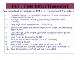
FET is a "Unipolar" device that depends only on the conduction of electrons (N-channel) or holes (P-channel).
Objectives • Explain the operation and characteristics of junction field effect transistors (JFET). • Understand JFET parameters. • Discuss and analyze how JFETs are biased. • Explain the operation and characteristics of metal oxide semiconductor field effect transistors (MOSFET). • Discuss and analyze how MOSFET are biased. • Troubleshoot FET circuits.
Introduction • FET – a three-terminal voltage-controlled device used in amplification and switching application. • BJT is a current-controlled device. • BJT uses input current flowing into the Base terminal to control the output Collector current of the transistor. • FET is a voltage-controlled device. • FET uses voltage in between two of the terminals (gate and source) to control current flow. • The FET’s major advantage over the BJT is high input resistance (thousand of Ohms) makes them very sensitive to input voltage signals, but they can be easily damaged by static electricity.
6.1. JFET • The JFET (junction field effect transistor) uses voltage to control the current flow. • The JFET is always operate with a reverse-biased pn-junction to control current in a channel. • JFETs can be used as an amplifier just like the BJT. • A JFET can be: p-channel and n-channel. • The terminals of a JFET: Source (S), Gate (G), and Drain (D).
The N-channel JFET's channel is doped with donor impurities meaning that the flow of current through the channel is -ve (hence the term N-channel) in the form of electrons. • The P-channel JFET's channel is doped with acceptor impurities meaning that the flow of current through the channel is +ve (hence the term P-channel) in the form of holes. • N-channel JFET's have a greater channel conductivity (lower resistance) than their equivalent P-channel JFET, since electrons have a higher mobility through a conductor compared to holes. • This makes the N-channel JFET's a more efficient conductor compared to their P-channel counterparts.
VDD provide a drain-to-source voltage. VGG sets the reverse-bias voltage between gate and source. JFET is always operated with gate-source pn-junction reverse-biased. Reverse-biasing of the GS-junction with a –ve gate voltage produces a depletion region along pn-junction. The depletion region extends into the n-channel and thus increases its resistance by restricting the channel width. The channel width and channel resistance can be controlled by varying the gate voltage. Thereby the amount of drain current (ID) flowing through the channel between the Drain and the Source terminals is controlled by a voltage applied to the Gate terminal, which is a reverse-biased. Basic Operation N-channel
N-channel JFET, Gate voltage is -ve. • P-channel JFET, Gate voltage is +ve. • JFETs are therefore known as depletion mode devices. • P-type region diffused into the N-type channel forming a reverse biased PN-junction and this junction forms the depletion region around the Gate area when no external voltages are applied. • This depletion region produces a potential gradient which is of varying thickness around the PN-junction and restrict the current flow through the channel by reducing its effective width and thus increasing the overall resistance of the channel itself.
6.2. JFET Characteristics and Parameters • Case: when the gate-to-source voltage, VGS=0V.This is produced by shorting the gate to source and both are grounded. • As VDD (and thus VDS) ↑ from 0V, ID will ↑ proportionally (as shown between point A and B).
JFET Drain Curve Point A to B: (Ohmic region) • ID↑ proportionally with increases of VDD (VDS↑ as VDD↑). • The channel has small depletion region, which is not large enough to have significant effect. ID will flow through from Drain to Source. • VDS and ID are related by Ohm’s Law.
Pinch-off voltage, VP • For VGS=0V, the value of VDS at point B is call Pinch-off voltage (VP) where the depletion is large enough. • At VP, the almost constant drain current (IDSS) begin. • ↑ in VDS above the VP produces an almost constant drain current (IDSS). • IDSS(Drain to Source current with gate Shorted)is the maximum drain current that a specified JFET can produce, and always specified for the condition, VGS=0V.
Point B to C: (constant-current area) • The curve levels off, ID becomes constant. • Because, as VDS↑, the reverse-bias voltage from gate to drain (VGD) produces a depletion region large enough to offset the increase in VDS.
Point C: (Breakdown) • Breakdown occur when ID begins to increase rapidly with any increase in VDS. • Breakdown result in irreversible damage to the device. • So JFETs operation is always well below this value.
VGS Controls ID • Case: As VGS is set to more –ve value by adjusting VGG. • A family of drain characteristic curves is produced.
For each in ↑ VGS, JFET reaches pinch-off at values of VDS less than VP. • JFET must be operated between VGS=0V and VGS(off). • The amount of ID is controlled by VGS. • The more -ve VGS, the smaller ID becomes because of the narrowing of the channel.
Cutoff Voltage, VGS(off) • Cutoff voltage, VGS(off) : The value of VGS (a very large –ve value) that makes ID ≈ 0. • When VGS(off) (a very large –ve value), ID≈ 0. • When VGS=0, ID= maximum IDSS. • Pinch-off voltage (Vp) and cutoff voltage (VGS(off)) are both the same value, but opposite in sign. • Example:VGS(off)= -5V, then VP = +5V.
N-channel JFET P-channel JFET
Example: For the JFET in Figure, VGS(off) = -4V and IDSS = 12mA. Determine minimum value of VDD required to put the device in the constant-current region of operation when VGS = 0V.
JFET Transfer Characteristic • For n-channel JFET, VGS(off) is –ve. • For p-channel JFET, VGS(off) is +ve. • Transfer characteristic curve (blue) can be developed from drain characteristic curves (green) by plotting values of ID for the values of VGS taken from the family of drain curves at pinch-off.
When VGS = - 2V, ID = 4.32mA. • When VGS = 0V, ID = IDSS = 12mA.
A JFET transfer characteristic curve is expressed approximately as: ID can be determined for any VGS if VGS(off) and ID are known. VGS(off) and ID are usually available from the datasheet
EXAMPLE The partial datasheet below for a 2N5459 JFET indicates that typically IDSS = 9mA and VGS(off) = -8V (maximum). Using these values, determine the drain current for VGS = 0V, -1V and -4V.
For VGS = 0V: For VGS = -1V: For VGS = -4V:
EXERCISE Determine ID for VGS = -1V, -3 V and -5 V for the 2N5457 JFET. Then draw transfer characteristic curve. Ans: From datasheet: IDSS = 3mA, VGS(off) = -6V VGS = -1V, ID = 2.083mA VGS = -3V, ID = 0.75mA VGS = -5V, ID = 0.083mA
JFET Forward Transconductance • Forward transfer conductance, gm is the changes in drain current (ΔID) based on changes in gate-to-source voltage (ΔVGS) with VDS is constant.
At VGS = 0, the minimum transfer conductance, gm0 can be calculated using: • By given gm0, calculate an approximate value for gm using: • gm0 can be read from the datasheet as gfs or yfs and sometimes written as Forward Transfer Admittance.
EXAMPLE For a 2N5457 JFET, typically IDSS = 3mA, VGS(off) = -6V maximum and Ȣfs(max) = 5000µS. Using these values, determine the forward transconductance for VGS = -4V and find ID at this point.
Ȣm0 = Ȣfs(max) = 5000µS VGS(off) = -6V VGS = -4V IDSS = 3mA
Input Resistance • Since JFET operates with GS-junction reverse-biased, which makes the input resistance (Rin) becomes so large at the gate. • This Rin can be calculated using : • IGSS : gate reverse current. • As IGSS increases with temperature, RIN will decrease. **Example 1: • Calculate RIN if IGSS= -2nA and VGS= -20V **Solution:
6.3. JFET Biasing • BJT and JFET must be biased for proper operation. • Four types of bias circuits: (1). self-bias, (2). gate-bias, (3). voltage-divider bias, (4). current-source bias.
(1). Self-Bias • Self-bias is the most common type of biasing method for JFETs. • Gate voltage, VG=0V. • To keep the GS-junction reverse biased: (a). VGS will be -ve for n-channel JFET, (b). VGS will be +ve for p-channel JFET. • Self-biased JFETs: ID = IS for all JFET circuits.
For n-channel JFET • IS through RS produces a voltage drop, making the Source +ve with respect to ground. • Since, IS = ID and VG = 0, VS = IDRS. • So: VGS = VG – VS = 0 - IDRS For p-channel JFET • IS through RS produces a –ve voltage at Source, making the Gate +ve with respect to ground. • Since, IS = ID, and VG = 0, -VS = –IDRS VGS = VG – (– VS ) = 0 – (– IDRS)
Keep in mind that analysis of p-channel is the same as n-channel except for opposite polarity voltages. • The drain voltage (VD) with respect to ground is: • Since VS = IDRS, VDS is:
EXAMPLE Find VDS and VGS if the drain current, ID of approximately 5mA is produced.
For VDS: For VGS:
EXERCISE Determine VDS and VGS when ID = 8mA. Ans: VS = 3.12 V VD = 5.12 V VDS = 2 V VGS = -3.12 V
Setting Q-Point: (Self-Bias) • Setting the Q-point requires us to determine a value of RS that will give us the desired IDand VGS. • For a desired value of VGS,IDcan be determinedfrom the: (a). Transfer characteristic curve (b). Formula: The data sheet provides the IDSS and VGS(off).
EXAMPLE Determine the value of RS required to self bias a n channel JFET with IDSS = 10mA and VGS(off) = -15V. VGS is to be -5V.
Midpoint Bias • Midpoint biasing- desirable to bias a JFET near the midpoint of its transfer characteristic curve where ID = 0.5IDSS. • ID = 0.5IDSSwhen:
To set the drain voltage at midpoint : (select a value of RD to produce the desired voltage drop.) • The value of RD needed can be determined by taking half of VDDand dividing it by ID:
The purpose of biasing is to set a dc operating point (Q-point). • In a self-biasing type JFET circuit, the Q-point is determined by the given parameters of the JFET itself and values of RS and RD. • Setting it at midpoint on the drain curve is most common. • RG, it’s value is arbitrary large to prevent loading on the driving stage in a cascaded amplifier arrangement.
EXAMPLE By referring datasheet, select resistor value for RD and RS to set up an approximate midpoint bias. Use minimum datasheet values when given; otherwise, VD should be approximately 6V(one-half of VDD) Ω
From datasheet: IDSS(min) = 1mA and VGS(off)(min) = -0.5V For midpoint bias: For RS:
For RD: From question, VD = 6V Kvl: -VDD+VRD+VD = 0
Biasing-graphical (Self-Bias) • The transfer characteristic curve along with other parameters can be used to determine the Q-point (ID and VGS) of a self-biased JFET circuit. • First, establish dc load line by calculating VGS when ID=0. VGS=-IDRS = (0)(470Ω) = 0 V **(ID=0, VGS=0)
Next, calculate VGS when ID=IDSS. VGS=-IDRS = (10mA)(470Ω) = -4.7V **(ID=10mA, VGS=-4.7V) • With 2 points, draw dc load line on the transfer characteristic curve. • The point where the line intersect the transfer characteristic curve is the Q-point of the circuit.