J-FET (Junction Field Effect Transistor)
J-FET (Junction Field Effect Transistor). Introduction

J-FET (Junction Field Effect Transistor)
E N D
Presentation Transcript
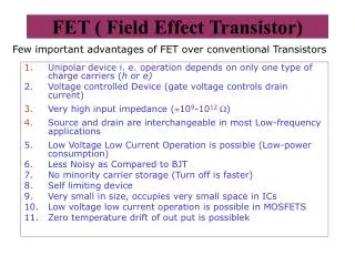
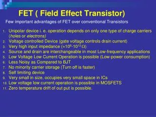
J-FET (Junction Field Effect Transistor) Introduction The field-effect transistor (FET) controls the current between two points but does so differently than the bipolar transistor. The FET operates by the effects of an electric field on the flow of electrons through a single type of semiconductor material. This is why the FET is sometimes called a unipolar transistor.
J-FET (Junction Field Effect Transistor) Current moves within the FET in a channel, from the source (S) connection to the drain (D) connection. A gate (G) terminal generates an electric field that controls the current . The channel is made of either N-type or P-type semiconductor material; an FET is specified as either an N-channel or P-channel device Majority carriers flow from source to drain. In N-channel devices, electrons flow so the drain potential must be higher than that of the Source (VDS > O)- In P-channel devices, the flow of holes requires that VDS < 0 Introduction…cont
JFET Construction A schematic representation of an n channel JFET is shown in Figure 118. An n-type channel is formed between two p-type layers which are connected to the gate. Majority carrier electrons flow from the source and exit the drain, forming the drain current. The pn junction is reverse biased during normal operation, and this widens the depletion layers which extend into the n channel only (since the doping of the p regions is much larger than that of the n channel). As the depletion layers widen, the channel narrows, restricting current flow.
J-FET (Junction Field Effect Transistor) The behavior of a JFET can be described in terms of a set of Characteristic Curves shown here. In the region shown with a green background the drain-source voltage is small and the channel behaves like a fairly ordinary conductor. In this region the current varies roughly in proportion to the drain-source voltage as if the JFET obeys Ohm's law. However, as we increase the drain-source voltage and move into the region with a light background we increase the drain-channel voltage so much that we start to ‘squeeze down’ the channel. Introduction…contd.
J-FET (Junction Field Effect Transistor) Hence a large increase in drain-source: • ‘pulls harder’, trying to drag the electrons more quickly from source to drain. • ‘squeezes down’ the channel making it harder for the electrons to get through. • These effects tend to cancel out, leaving the current the same at all high drain-source voltage.