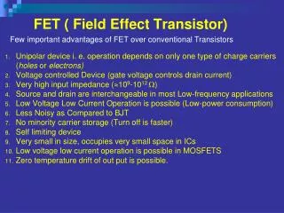
Field Effect Transistor (FET)
Field Effect Transistor (FET). Introduction. Field Effect Transistor (FET). Junction Field Effect Transistor (JFET). Metal Oxide Semiconductor FET (MOSFET). Depletion Type MOSFET. Enhancement Type MOSFET. Junction Field Effect Transistor (JFET). n-channel JFET. p-channel JFET.


Field Effect Transistor (FET)
E N D
Presentation Transcript
Introduction Field Effect Transistor (FET) Junction Field Effect Transistor (JFET) Metal Oxide Semiconductor FET (MOSFET) Depletion Type MOSFET Enhancement Type MOSFET
Junction Field Effect Transistor (JFET) n-channel JFET p-channel JFET
JFET Introduction • JFET is always operated with the gate source p-n junction reversed biased.
JFET Introduction Channel width and thus the channel resistance can be controlled by varying the gate voltage. JFET biased for construction Greater VGG narrows the channel Water analogy for the JFET control Less VGG widens the channel
JFET Characteristics and Parameters • For VGS = 0 v, the value of VDS at which ID becomes essentially constant is the pinch-off voltage (Vp) and is denoted as IDSS. • Breakdown occurs at point C when ID begins to increase very rapidly with any further increase in VDS .
VGS controls ID. The value of VGS that makes ID approximately zero is the cutoff voltage VGS(off). The JFET must operate between VGS = 0 and VGS(off) .
Transfer Characteristics • William Bradford Shockley derived a relationship between ID and VGS which is known as Shockley’s equation and is given by • The above equation suggests that • when VGS = 0, ID = IDSS. • When VGS = Vp, ID = 0
Example The following parameters are obtained from a certain JFET datasheet: VP = -8 v and IDSS = 5 mA. Determine the values of ID for each value of VGS ranging from 0 v to -8 v in 1 v steps. Plot the transfer characteristic curve from these data. Solution:
ID VGS
FET Biasing • The following relations can be applied to the dc analysis of most of the FET amplifiers:
JFET Biasing: Fixed Bias Circuit Circuit for dc analysis
Fixed Bias Circuit GS Loop: • Apply KVL • Apply the Shockley’s Equation: • Plot Shockley’s equation:
Fixed Bias Circuit • Q-Point:
Fixed Bias Circuit • DS Loop Also note that In addition
Example: Determine the following for the given Fig. • VGSQ (b) IDQ (c) VDS (d) VD (e) VG (f) VS. Solution: (a) VGSQ = -VGG = -2 V (b) (c) (d) VD = VDS = 4.75 V (e) VG = VGS = -2 V (f) VS = 0 V
Self Bias Circuit: DC Analysis Self-bias Circuit for dc analysis
JFET Self Bias Circuit IG = 0 IS = ID From GS Loop: -VGS = VRS or VGS = -ISRS Substituting IS = ID VGS = -IDRS.
JFET Self Bias Circuit Shockley Equation:
JFET Self Bias Circuit: Q-Point Transfer Curve (Shockley equation) Self-Bias Line: Since VGS = -IDRS . If ID = 0 then VGS = 0 and ID = IDDS/2 (say), then VGS = -IDDS RS /2 Superimposing this straight line on the transfer curve, we get Q-point as shown in the Fig. Self Bias line
JFET Self Bias Circuit DS Loop: Using KVL Substituting IS = ID, or In addition
JFET Self Bias Circuit: Example 1 Determine the following: VGSQ , IDQ, VDS, VS, VG, and VD. Solution: Step 1: Draw the self bias line: VGS = - IDRS , When ID = 0, VGS = 0. Choosing ID = 4 mA, VGS = -4mA×1 k = -4 v The line is drawn below:
JFET Self Bias Circuit: Example 1 Step 2: Plot the Shockley equation: (IDSS = 8mA, VP = -6v) ID (mA) VGS (volts)
JFET Self Bias Circuit: Example 1 Step 3: Show the Shockley curve and the self bias line on the same graph paper Shockley Curve Q-Point ID (mA) Self bias line VGS (volts) From the graph, VGSQ = -2.6 v, IDQ = 2.6 mA
JFET Self Bias Circuit: Example 1 Step 4: Find the remaining quantities: VDS = VDD – ID(RS + RD ) = 20 – 2.6mA( 1 k + 3.3 k) = 8.82 v VS = IDRS = (2.6mA)(1k) = 2.6 v VG = 0 v VD = VDS + VS = 8.82 + 2.6 = 11.42 v (or VD = VDD – IDRD = 11.42 v)
JFET Biasing: Voltage Divider Circuit dc analysis Applying KVL, VG or But VRS = ISRS = IDRS Therefore
Voltage Divider Circuit: Q-Point Bias Line: (i) When ID = 0 VGS = VG – IDRS = VG – (0)(RS) VGS = VG (ii) When VGS = 0 Plot this line along with the Shockley Curve, as shown in the Figure.
JFET Biasing: Voltage Divider Circuit dc analysis From DS Loop: VG
Voltage Divider Circuit: Example Determine the following: • IDQ and VGSQ. • VD • VS • VDS • VDG.
Voltage Divider Circuit: Example 1 Solution: IDSS = 8 mA, Vp = -4 v. Shockley Equation: Bias Line: When ID = 0, VGS = 1.82 v For VGS = 0, ID = 1.82/1.5k = 1.21 mA
From the Figure, IDQ = 2.4 mA, VGSQ = -1.8 v VD = VDD - IDRD = 16 – (2.4mA)(2.4k) = 10.24 v (c) VS = IDRS = 16 – (2.4mA)(2.4k) = 10.24 v (d) VDS = V DD – ID(RD + RS ) = 16 – (2.4mA)(2.4k + 1.5k) = 6.64 v (e) VDG = VD - VG = 10.24 – 1.82 = 8.42 v
Voltage Divider Circuit: Example 2 For the given network, Detrmine • VG. (b) IDQ and VGSQ. • VD and VS. • VDSQ . Solution: (a) (b) IDSS = 10mA, Vp = -3.5 v
Bias Line:VGS = VG – IDRS = 2.16 – ID(1.1k) When ID = 0, VGS = 2.6 v When VGS = 0, I = 2.16/1.1k = 2mA From the graph, we see that IDQ = 3.3 mA, VGSQ = -1.5 v (c) VD = VDD – IDQRD = 20 - (3.3mA)(2.2k) = 12.74 v VS = IDRS = 3.63 v (d) VDSQ = VDD – IDQ(RD +RS ) = 9.11 v
Metal-Oxide -Semiconductor Field Effect Transistor (MOSFET) MOSFET Depletion –Type MOSFET Enhancement-Type MOSFET
N- Channel Depletion-Type MOSFET • The foundation of this type of FET is the substrate (p-type material). • The source and drain terminals are connected through metallic contacts to n doped regions linked by an n channel. • The gate is also connected to a metal contact surface but remains insulated from the n-channel by a SiO2 layer. Construction of D-MOSFET (n-Channel)
Basic Operation and Charactersitics of N – Channel D-MOSFET • When VGS = 0 and VDS is applied, the drain current ID = IDSS flows through the circuit due to the free electrons of the n-channel. VGS = 0 I D= I S= IDSS
Basic Operation and Characterstics of N-Channel D-MOSFET • When VGS < 0, recombination between electrons and holes occurs. The more negative the bias, the higher the rate of combination. The resulting level of ID is reduced and becomes zero at pinch-off voltage. Electrons repelled by negative Potential at gate.
Basic Operation and Charactersitics of D-MOSFET • When VGS > 0, the gate will draw additional electrons from the p-substrate due to the reverse leakage current and the drain current increases at a rapid rate.
Example: Sketch the transfer characteristics for an n-channel depletion type MOSFET with IDSS = 10 mA and Vp = -4 v. Solution: The curve is plotted on the next slide.
Drain Current (A) Gate Source Voltage
Symbols P-Channel N-Channel
18 v Example1: For the n-channel depletion type MOSFET of the Fig., determine (a) IDQ and VGSQ. (b) VDS. Solution: Shockley Equation:
Bias Line: When ID = 0, VGS = 1.5, When VGS = 0, ID = VG/RS = 1.5/750 = 2 mA From the graph, IDQ = 3.1 mA, VGSQ = -0.8 v VDS = VDD – ID(RD + RS) = 10.1 v
Example2: Determine the following for the given network. (a) IDQ and VGSQ (b) VD. Solution: (a) Shockley Equation: