FET (Field effect transistor)
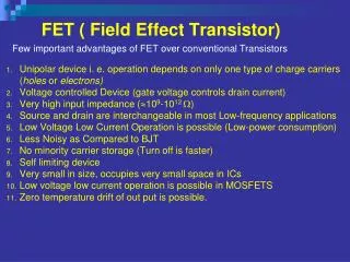
FET (Field effect transistor). Two main groups JFET (junction FET) MOSFET (metal-oxide-semiconductor FET) Advantage extremely large input impedance Disadvantages Smaller gain (g m ) than bipolar transistor More difficult to analyze. Drain. I. Gate. Source. JFET. n-channel JFET

FET (Field effect transistor)
E N D
Presentation Transcript
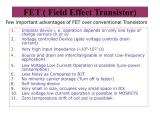
FET (Field effect transistor) • Two main groups • JFET (junction FET) • MOSFET (metal-oxide-semiconductor FET) • Advantage • extremely large input impedance • Disadvantages • Smaller gain (gm) than bipolar transistor • More difficult to analyze
Drain I Gate Source JFET • n-channel JFET • just a slab of n-type semiconductor !! • like transistor, the drain current is controlled by VGS FET Bipolar Gate = base Source = emitter Drain = collector
JFET • n-channel JFET • PN junction • reversed biased
JFET operation VG=0 VD • VGS=0 • Max conducting channel, max drain current ID • VT <VGS < 0 • pn junction is reverse biased • reduce the conducting channel • reduce the drain current • VGS < VT (Pinch-off voltage) • Further reduce VGS until the depletion layer grows so wide that the channel is completely blocked • ID=0 VS=0 P N ID VT <VG<0 VD VS=0 VG< VT VD VS=0
JFET as a voltage-controlled resistor • If VDS is small • VGS controls the channel width, and therefore the resistance • JFET is a voltage-controlled resistor VG VD VS
VG= -2V VD = 5V VS=0 P N-channel JFET as a voltage-controlled current source • If VDS is large • the drain end is more reversed biased ! • The channel is warped • Increase VDS => increase depletion => reduce ID • But increase VDS=> increase ID • Net result • ID remains constant even VDS is increased • A voltage-controlled current source
Saturation region • Small VDS - linear region (voltage controlled resistor) • Large VDS – saturation region (constant ID, voltage controlled current source) Linear region Small VDS JFET is like a resistor
ID vs VGS (saturation region) • IDSS • maximum current at VGS=0 (widest channel width, smallest resistance) • different FET has different IDSS IDSS VP
ID vs VGS • The slope of ID vs VGS (gm) is less steep (not an exponential) • smaller gm, not as good as bipolar transistor • FET is difficult to analyze • Bipolar is easier to analyze because VBE ~ 0.6V • VGS can vary over a wide range, usually analyze by graphical method (load-line) • The most important advantage • Input is connected to an reversed biased pn junction • Extremely high input impedance (IG~0)
FET versus bipolar • FET is similar to bipolar transistor • Voltage-controlled current source • bipolar circuits can be used by FET
VDS A simple current source • What is VGS? • What is ID? • The simplest current source ! • But we cannot choose the current, as IDSS mayvary from transistor to transistor
An adjustable current source • Add a resistor RS so as to adjust ID • Find by load-line (graphical) method VSG= IDRS VGS= -IDRS
gm of FET Curve approx by a parabola VT
k can be found by measuring gm at two points • At VGS=0, measure gm (gm is maximum) • Find VT (corresponds to gm=0)
Typical value of gm at ID=1mA • JFET ~ 2m A/V (from data book) • bipolar ~ 40m A/V (by calculation gm=IC /25mV) • Gain of bipolar is much higher than FET ! • Why use FET? • extremely high input impedance • almost zero input current • good for picking up signal from source that has high source impedance • e.g. microphones, input stage of oscilloscope
Source Follower • Same as emitter follower • Output voltage (VS) follows input (VG) • DvG , DiD , DiDRS , DvS
Source Follower • AC signal analysis • if RSgm >> 1, then DVG ~ DVS=> good follower • To have large RS, use current source (active load)
Output impedance • Fixed gate voltage, what is the output impedance • model the gate-source section by a resistor • DvOUT / DiD = rS = 1/gm (because DvOUT ~ DVIN) • Typical value • gm ~ 2m A/V, therefore rS ~ 500W • The output impedance of source follower (500W) is much higher than emitter follower (25W)
Matched FET follower • The follower is made of matched FET • Q2 is a current source at VGS=0 and ID2=IDSS • Q1 and Q2 are matched, • Since ID1 = ID2 , therefore VGS1= VGS2 = 0V (!) • zero DC offset
FET amplifier • DvG , DiD , DvOUT = -RDDiD • input and output are 180o out of phase, just like bipolar amplifier • gain • DiD = gmDvGS • DvD = -RDDiD = -gmRDDvGS • voltage gain = -gmRD • same as bipolar amp except gm is smaller
FET amplifier • DC bias • VGS = -ID R • use load-line to find the best R for VGS and ID R
Hybrid op amp - best of both worlds The tail, large impedance gives high CMRR Push-pull class B amp Mirror as active load. High gain amplifier Follower as buffer
Voltage Regulators • Input: unregulated power supply (voltage is quite constant but still has some ripple) • Output: regulated (constant) voltage
Voltage Regulator • Regulator = Voltage reference + follower • unregulated input provides the power • zener diode (Vref) provides the voltage reference • follower provides the output power and current
Dropout voltage • Dropout voltage • difference between input and output voltage
Dropout voltage • For 723 • supply voltage of 9.5V (min) produces 5V output • Large 4.5V dropout voltage (not good), waste power • also requires too many external components • Modern regulators • dropout voltage ~ 2-3V • Specialized low-dropout regulators • dropout voltage ~ a few tenths of a volt
78xx family • A modern regulator that you would use • only need to provide a couple smoothing capacitors
High current output • Use parallel transistors to give high output current
Thermal runaway • Consider the bipolar transistors • different discrete transistor has different IC vs VBE curve • if one transistor conducts more current than the other • the transistor gets hotter • conduct more current !! • which makes the transistor hotter still, develops a local hot spot, may eventuallybreak down
Thermal runaway • The use of the resistor R in the emitter follower • Negative feedback • If a transistor gets hot and conducts more current • VE is increased, providing a feedback voltage so that VBE is reduced, which reduces the current • FET does not have the problem of thermal runaway • Because FET has –ve temperature coefficient • Increase in temperature reduces output current • Really large power amplifiers can be built using MOSFET as the output stage
Switching regulators • Regulators powered by microprocessors • run at 75%-90% efficiency, more efficient than traditional regulators • transformer-less (so that the size is small) • but more noisy (high frequency noise) • Work by dumping charges into a capacitor via a switch • charges stored in the capacitor give a constant voltage
Switching regulators Dump charge to cap
MOSFET (Metal Oxide Semiconductor FET) • Any current in the circuit below? • No current • one end must be reversed biased n n p
MOSFET • Basic principle - capacitive effect metal +++++++++++++ - - - - - - - - - - - - - charge
Enhancement MOSFET • Add a metal gate • Capacitive effect builds up a –ve charge channel that allows electrons to flow metal insulator gate n n - - - - - - - - - - - - source drain p body -ve charge, conducting channel
NMOS (n-channel MOS) • when gate voltage is zero, no drain current • drain current increases as gate voltage increased
Enhancement mode and depletion mode • Enhancement mode operation • No gate voltage, no conduction • Increase gate voltage increases the conduction • JFET • Depletion mode • no gate voltage, conduction is at its maximum
Enhancement MOSFET • if VDS is small • VGS controls channel width • IDS VDS • behaves as a variable resistor • Large VDS • VDS increase, drain becomes more positive • conducting channel becomes less -ve charged to the point that it will almost be vanished • Channel is warped • Saturation • increase in VDS also increase drain current but offset by the reduction in channel • Constant ID over a range of VDS 3V 5V - - - - - - - - - 0V warped
With PMOS (p-channel MOS) • Works in opposite polarity
Digital circuits • Logic gates • the fundamental building block of digital electronics • AND, OR, NAND, NOR, INVERTER • with these gates, one can build adder, shifter, multiplier, logical unit, memory, and microprocessors
Inverter gate • NMOS (n-channel MOSFET) inverters Output impedance at OFF state VOUT ON. Channel is conducting, drain is shorted to ground, VOUT = 0 OFF. Channel is non-conducting, ID=0, VOUT = VDD
Drawback of NMOS • ON state • draw current though R, large static power dissipation • OFF state • Large output impedance = R • Large R gives small output current, which slows the switching speed of the circuit
Problems of NMOS • Large RD-> takes longer to charge up Cstray
CMOS inverter (Complementary MOSFET) • PMOS + NMOS • Input = 0V, Output = 5V • for NMOS (bottom one) • VGS=0V, OFF • (open circuit) • for PMOS • VG= 0V, VS= 5V • VGS= -5V, ON • (Short circuit) (5V) VGS = -5V VGS = 0V
CMOS inverter (Complementary MOSFET) • PMOS + NMOS • Input = 5V, Output = 0V • for NMOS (bottom one) • VGS=5V, ON • (short circuit) • for PMOS • VGS= 0V, OFF • (open circuit) (5V) VGS = 0V VGS = 5V
CMOS • Output impedance • Either the PMOS or the NMOS is short • Zero W , tiny RC, fast switching • Static power consumption • output = 5V • NMOS (bottom) is open circuit, draw no current • PMOS is short, draw no voltage • Power = VI = 0 • output = 0V (same, power=0) • ideal for low power applications • e.g. mobile phone, notebook PC
Dynamic power dissipation • Dynamic power dissipation • Power consumes when there is a change of state • 0 -> 1 or vice versa • CMOS draws power when the MOSFET is changing state • Both MOSFETs are partially conducting • Charging up the stray capacitor of next stage consumes energy