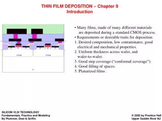
Thin Film Deposition
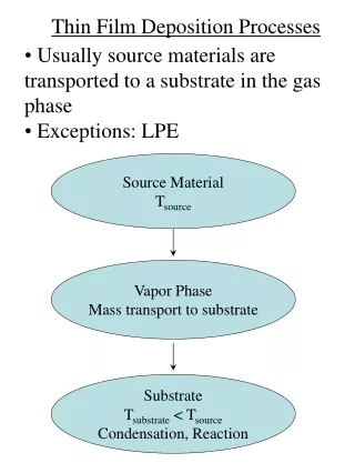
Thin Film Deposition. Topics: Chemical Vapor Deposition Physical Vapor Deposition Evaporation Sputtering Strengths and Weaknesses Basic Calculations. Issues related to thin film deposition. Quality: Composition Defect density (e.g. pinholes) Contamination

Thin Film Deposition
E N D
Presentation Transcript
Thin Film Deposition • Topics: • Chemical Vapor Deposition • Physical Vapor Deposition • Evaporation • Sputtering • Strengths and Weaknesses • Basic Calculations
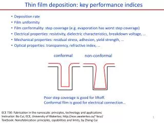
Issues related to thin film deposition • Quality: • Composition • Defect density (e.g. pinholes) • Contamination • Mechanical and electrical properties • Good adhesion • Minimum stress • Topography • Uniform thickness on non-planar surfaces • Step coverage • Conformal coverage: uniform • Space filling in holes, channels • Voids
Thin film filling issues: (a) shows good metal filling of a via or contact hole in a dielectric layer (b) silicon dioxide dielectric filling the space between metal lines, with poor filling leading to void formation (c) poor filling of the bottom of a via hole with barrier or metal SEM photo showing typical coverage and filling problems
Two types of thin film deposition: CVD and PVD • CVD • Reactive gases interact with substrate • Used to deposit Si and dielectrics • Good film quality • Good step coverage • PVD • Used to deposit metals • High purity • Line of sight
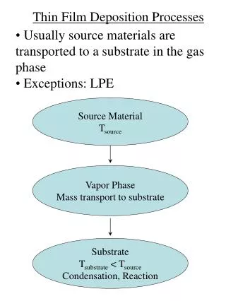
CVD Gases react with substrate Various types of CVD: Atmospheric pressure – APCVD Low pressure – LPCVD Plasma enhanced – PECVD High density plasma - HDPCVD • CVD systems • APCVD w/cold wall for deposition of epitaxial silicon • LPCVD w/hot wall for depositing polycrystalline and amorphous silicon
Steps in CVD • Transport reactants via forced convection to reaction region • Transport reactants via diffusion to wafer surface • Adsorb reactants on surface • Surface processes: chemical decomposition, surface migration, site incorporation, etc. • Desorption from surface • Transport byproducts through boundary layer • Transport byproducts away from deposition region
Flux through boundary layer: F1 = hG(CG-Cs) (molecules/cm2/s) Flux of reactants consumed at surface: F2 = ksCs(molecules/cm2/s) Process is limited by slowest step, thus F = F1 = F2
Film Growth Define Y = CG/CT = PG/Ptotal If ks << hG, then v ≈ CT/N ksY If hG<< ks, then v ≈ CT/N hGY ks = hGexp(-Ea/kT) Ea ≈ 1.6 eV
hG = DG/ds The position of the boundary layer changes wrt x: Boundary layer velocities along susceptor. ds is the thickness of the boundary layer. The boundary layer increases with distance in the direction of gas flow m = viscosityr = density of gasU = gas velocity The susceptor in a horizontal epitaxial reactor is tilted so that the cross-sectional area of the chamber is decreased, increasing the gas velocity along the susceptor. This compensates for both the boundary layer and depletion effects.
Autodoping Gases may be doped, e.g., AsH3, PH3, B2H6 Autodoping occurs when dopant atoms adsorbed on (1) wafer frontside (2) wafer backside and edges (3) other wafers and (4) susceptor are reemitted.
LPCVD Recall that: Growth velocity vs 1/T for APCVD (760 torr) and LPCVD (1 torr) systems. The lower total pressure (with PG and CG fixed) shifts the hG curve upward, extending the surface reaction regime to higher temperatures. Decreasing Ptotal increases DG, hG and v
Advantages of LPCVD • Faster growth • Less autodoping • Little diluent gas needed • Lower gas consumption • Fewer byproducts (particles) • Disadvantages: • Line of sight • Poorer step coverage • shadowing
Plasma Enhanced CVD (PECVD) Good when temperature is restricted Provides reasonable deposition rates Good film quality Conformal May leave unwanted byproducts on film
Physical Vapor Deposition: PVD 2 types: evaporation and sputtering Advantages: Versatile – deposits almost any material Very few chemical reactions Little wafer damage Limitations: Line-of-sight Shadowing Thickness uniformity Difficult to evaporate materials with low vapor pressures
Flux from a point source Deposition rate from a surface source: Geometries of flux and deposition of small areas on a flat wafer holder for (a) a point source and (b) a small planar surface source
Deposition rate of evaporated film as function of position on substrate for point and surface sources. qi = qk in this configuration for both point and surface sources.
Mean free path l: k = 1.36 x 10⁻² erg/at-K d≈.4 x 10-8 cm Pe = partial pressure (torr) Vapor pressure as a function of temperature of commonly evaporated metals
Sticking coefficient: Sc = Freacted/Fincident The depositing species have a high sticking coefficient (close to 1) in (a), so that they are deposited where they first strike. In (b) the depositing species have a low sticking coefficient (<<1) so that man are reemitted and deposit elsewhere on the topography, such as the sidewalls.
Sputtering Schematic diagram of DC-powered sputter deposition equipment Plasma structure and voltage distribution in DC sputter system
Distribution of arrival fluxes for (a) uniform or isotropic arrival distribution and (b) directed or anisotropic arrival distribution. Arrival angle distribution (cosnq) is defined by arrival flux relative to unit surface area. This flux is equal to the normal component of incoming flux, relative to the vertical direction for a horizontal surface. Processes in sputter deposition
Effect of arrival angle distribution of depositing species on filling trenches or holes. In (a) a relatively wide arrival angle distribution leads to poor bottom filling or coverage, while (b) a narrower arrival angle distribution leads to better bottom filling. The higher the aspect ratio of the feature, the narrower the arrival angle distribution must be for adequate coverage. Schematic diagram of ionized sputter deposition system (ionized PVD) showing atomic flux lines