Download
1 / 43
450 likes | 729 Vues
Atomic Scale Intermixing during Thin Film Deposition. 김상필 * , 유승석 § , 이승철 , 이규환 , 이광렬 한국과학기술연구원 , 미래기술연구본부 * 한양대학교 , 세라믹스 공학과 , § 서울대학교 , 재료공학부. 2004. 5. 21. 표면공학회 춘계학술대회 , 서울대학교. Nanoscience and Nanomaterials. Chracteristics of Nano Materials.

E N D
Atomic Scale Intermixing during Thin Film Deposition 김상필*, 유승석§, 이승철, 이규환, 이광렬 한국과학기술연구원, 미래기술연구본부 * 한양대학교, 세라믹스 공학과, § 서울대학교, 재료공학부 2004. 5. 21. 표면공학회 춘계학술대회, 서울대학교
Chracteristics of Nano Materials • Continuum media hypothesis is not allowed. • Large fraction of the atom lies at the surface or interface. • Abnormal Wetting • Abnormal Melting of Nano Particles • Chemical Instabilities
Nanoscience or Nanotechnology • To develop new materials of devices of novel properties by understanding a phenomenon in the scale of atoms or molecules and manipulating them in an appropriate manner. Needs Atomic Scale Understandings on the Structure, the Kinetics and the Properties
Scientific Computation & Simulationin (sub) Atomic Scale First Principle Calculation Molecular Dynamic Simulation
Case III : GMR Spin Valve Major Materials Issue is the interfacial structure and chemical diffusion in atomic scale
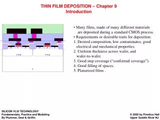
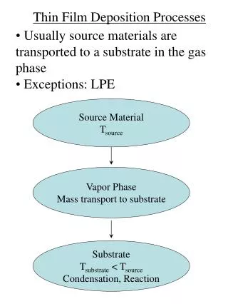
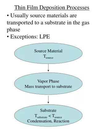
Conventional Thin Film Growth Model Conventional thin film growth model simply assumes that intermixing between the adatom and the substrate is negligible.
The Present Work • We employed the molecular dynamic simulation to understand the atomic scale phenomena during thin film process in spintronic devices. . • We focused on the interfacial intermixing behavior in atomic scale. Performance of spintronics devices are largely depends on theInterface Structuresof the Metal/Metal or Metal/Insulator
i Time Evolution of Ri and vi MD Simulation Interatomic Potentials Lennard-Jones: Inert Gas Embedded Atom Method: Metals Many Body Potential: Si, C
[001] z y x [010] [100] Adatom (0.1eV, normal incident) 300K Initial Temperature Substrate 300K Constant Temperature Fixed Atom Position Program : XMD 2.5.30 x,y-axis : Periodic Boundary Condition z-axis : Open Surface Atom flux : 5ps/atom MD calc. step : 0.5fs
FCC - Al HCP - Co EAM Potential for Co and Al * A. Voter et al. MRS Symp.Proc. , 175 (1987) ** R. Pasianot et al , PRB 45 12704 (1992)
EAM Potential for Co–Al CoAl B2 * Intermetallic Compound , Vol 1, 885 (1994) ** C. Vailhe et al. J. Mater. Res., 12 No. 10 2559 (1997) *** R.A. Johnson, PRB 39 12554 (1989)
Phase Diagram of Co-Al CoAl: B2
Deposition Behavior on (111) Al on Co Co on Al TOP VIEW
CoAl Structural Analysis • CoAl compound layer was formed spontaneously.
CoAl: B2 Al on Co Co on Al
Co on Al (100) 1.4 ML 2.8 ML 4.2 ML N.R. Shivaparan, et al Surf. Sci. 476, 152 (2001)
Energy Barrier for Co Penetration (3) (1) (2) (1) (3) (2) Reaction Coordinate • Activation barrier is larger than the incident kinetic energy (0.1eV) of Co. • How can the deposited Co atom get that sufficient energy to overcome the activation barrier?
1 3.5eV 2 3 4 Acceleration of Deposited Co Near Al Substrate Co Hollow site Al (1) (4) (2) (3)
Deposition Behavior on (001) Co on Al Al on Co
Al on Co (001) Contour of Acceleration Co on Al (001)
Reaction Coordinate Depostion Behavior on (001) Co on Al (001)
Deposition Behavior on (001) Al on Co (001)
Deposition Behavior on (001) Al on Al (001) Al on Al (100)
2ML Al on Co(001) B2-like on Co(001) Nano-scale Sandwich Structure Co/B2/Co A Suggested Novel Process
EAM Potential for Co-Cu system* * X. W. Zhou et al., Acta. Mater., 49, 4005 (2001).
0.1eV Co on Cu (001) 128 atoms 256 atoms 384 atoms Mixing Ratio : 1.56%
0.1eV Cu on Co (001) 128 atoms 256 atoms 384 atoms Mixing Ratio : 0.0 %
5.0eV Co on Cu (001) 128 atoms 256 atoms 384 atoms Mixing Ratio : 21.1%
5.0eV Cu on Co (001) 128 atoms 256 atoms 384 atoms Mixing Ratio : 0.78 %
Intermixing Behavior Cu on Co (100) Co on Cu (100)
Kinetic Energy of Co near Cu (100) Hollow site Top site 2.63 eV 1.81 eV
Comparison of Interatomic Potential Co-Al Co-Cu
Energy Barrier for Intermixing • Similar atomic radius induce a simple substitutional exchange.
Energy Barrier for Intermixing 1.21 eV 0.553 eV Co on Cu(001) Cu on Co(001)
Conclusions • In nano-scale processes, the model need to be extended to consider the atomic intermixing at the interface. Conventional Thin Film Growth Model Calculations of the acceleration of adatom and the activation barrier for the intermixing can provide a criteria for the atomic intermixing.