Download
1 / 10
140 likes | 332 Vues
Thin Film Semiconductor Deposition Market is segmented by deposition technology and industry verticals. Thin film market is expected to get $22 bn by 2022<br>https://www.alliedmarketresearch.com/thin-film-semiconductor-deposition-market<br>

E N D
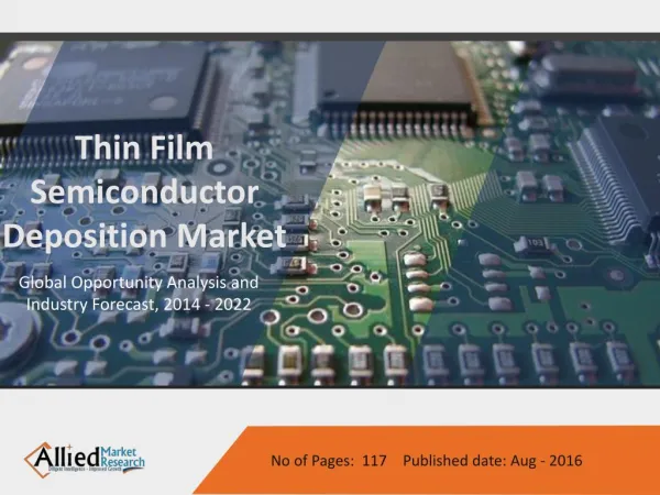
Thin Film Semiconductor Deposition Market Global Opportunity Analysis and Industry Forecast, 2014 - 2022 No of Pages: 117 Published date: Aug - 2016
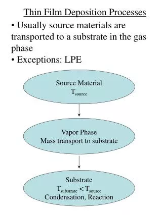
Introduction to Thin Film Semiconductor Deposition Market • Thin Film Semiconductor Deposition Market Report, published by Allied Market Research, forecasts that the global market is expected to garner $22 billion by 2022, registering a CAGR of 14% during the forecast period 2016 - 2022. • Thin films are extensively used in applications such as DRAM, solar panels, and flexible OLED & AMOLED displays. Moreover, increase in demand for efficiency and circuit miniaturization has supplemented the growth of TFS deposition market. • Thin film deposition technology is bifurcated into three types that include, chemical vapor deposition (CVD), physical vapor deposition (PVD), and others. • Among all, CVD technology holds a significant revenue share in the world TFS deposition market, owing to its low manufacturing cost, comparatively easier manufacturing process, and extensive use in fastest growing photovoltaic technology. • In addition, CVD technology is expected to witness the fastest growth during the forecast period, with a CAGR of 14.7%.
Introduction to Thin Film Semiconductor Deposition Market • The growth would be driven by increase in demand of microelectronic components, electronic devices, and its expanding usage in sensors for smartphones which are growing rapidly across the globe. • Among all industry verticals, electronics accounted the largest market share in overall TFS deposition market. • This is mainly due to increase in demand of thin film semiconductors in PCs, smartphones, and OLED displays. • Moreover, increase in demand for personal computers, electronic gadgets, and home appliances has supplemented the growth of TFS in electronics industry. • However, energy & power, is anticipated to witness the highest growth rate among others owing to increase in investment by various countries and replacement of conventional silicon by thin film semiconductors on the panels. • Asia-Pacific is the largest revenue-generating region in this market owing to the presence of largest electronic equipment producers and consumers in the region followed by North America and Europe.
Thin Film Semiconductor Deposition Market Key Segments Chemical Vapor Deposition (CVD) Deposition Technology Physical Vapor Deposition (PVD) Thin Film Semiconductor Deposition IT & Telecom Industry Vertical Electronics Thin Film Semiconductor Deposition Market Segments
Thin Film Semiconductor Deposition Market Dynamics Drivers • Technological Superiority of Thin Film Over Conventional Silicon • High Demand due to Increasing Usage in Emerging Applications Such As Dram, Flexible Oled Displays and Amoled Displays • Increasing Demand for Higher Efficiency And Miniaturization • Growing Investment in Solar Power Plants Restraints • High Initial Investment for Setting Up A Manufacturing Plant • Poisonous Properties of Cadmium Used in Thin Film Fabrication
Key Benefits of Thin Film Semiconductor Deposition Market • Comprehensive analysis of the current and future trends in the global thin film semiconductor deposition market has been provided in this report. • The report provides a competitive scenario of the thin film semiconductor deposition market along with the growth trends, structure, driving factors, scope, opportunities, and challenges. • The report includes a comprehensive analysis of the market segments to provide insights on the market dynamics. • Porters Five Forces analysis highlights the potential of buyers and suppliers as well as provides insights on the competitive structure of the market to devise effective growth strategies and facilitate better decision-making. • Value chain analysis provides key inputs on the role of stakeholders involved at various stages of the value chain.
Thin Film Semiconductor Deposition Market By Geography North America, Europe, Asia-Pacific, LAMEA
Key Players of Thin Film Semiconductor Deposition Market • Applied Materials • Tokyo Electron Limited • Lam Research • Shin-Etsu Chemical Co
Thank You! For More Details Visit us at Applied Materials, Tokyo Electron Limited, Lam Research, and Shin-Etsu Chemical Co., https://www.alliedmarketresearch.com/thin-film-semiconductor-deposition-market Follow Us On