Thin Film Deposition
370 likes | 1.06k Vues
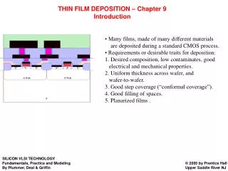
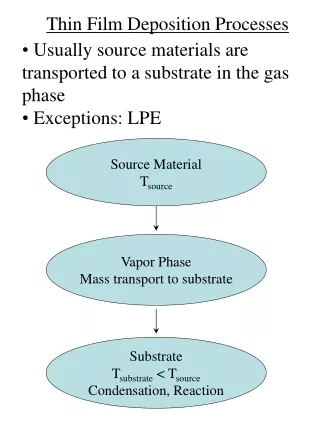
Thin Film Deposition. Quality – composition, defect density, mechanical and electrical properties Uniformity – affect performance (mechanical , electrical). Thinning leads to R.

Thin Film Deposition
E N D
Presentation Transcript
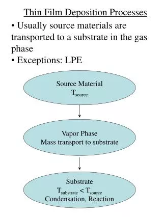
Thin Film Deposition • Quality – composition, defect density, mechanical and electrical properties • Uniformity – affect performance (mechanical , electrical) Thinning leads to R Voids: Trap chemicals lead to cracks (dielectric) large contact resistance and sheet resistance (metallization) AR (aspect ratio) = h/w with feature size in ICs. Plummer et al.
Chemical Vapor Deposition Methods of Deposition: Chemical Vapor Deposition (CVD), Physical Vapor Deposition (PVD: evaporation, sputtering) Cold wall reactor Atmospheric Pressure : APCVD Cold wall reactors (walls not heated only the susceptor) Flat on the susceptor Low pressure: LPCVD – batch processing. Hot wall reactor Plummer et al.
Plasma Enhanced Chemical Vapor Deposition(PECVD) • Used when : • Low T required (dielectrics on Al, metals) but CVD at decreased T gives increased porosity, poor step coverage. • Good quality films – energy supplied by plasma increases film density, composition, step coverage for metal decreases but WATCH for damage and by product incorporation. 13.56 MHz P 50 mtorr - 5 torr Plasma: ionized excited molecules, neutrals, fragments, ex. free radicals very reactive reactions @ the Si surface enhanced increase deposition rates Ions, electrons, neutrals = bombardment Outgassing , peeling , cracking stress. 200- 350 °C Plummer et al.
Physical Vapor Deposition (PVD) – no chemical reactions (except for reactive sputtering) Evaporation • Advantages: • Little damage • Pure layers (high vacuum) • Disadvantages: • Not for low vapor pressure metals • No in-situ cleaning • Poor step coverage Very low pressure (P < 10 –5 torr) - long mean free path. • purer – no filaments, only surface of the source melted • X-rays generated trapped charges in the gate oxides anneal it ! Plummer et al.
Evaporation Partial Pressure of the source (target) Needed for reasonable v 0.1 - 1m/min No alloys – partial pressure differences Use separate sources and e-beam • Step Coverage Poor : • Long mean free path (arrival angle not wide = small scattering) and low T (low energy of ad-atoms) • Sticking coefficient high (@ T) no desorption and readsorption poor step coverage • Heating can increase Sc but may change film properties (composition, structure) Sticking coefficient Plummer et al.
Sputter Deposition Higher pressures 1 –100 mtorr ( < 10-5 torr in evaporation) Major Technique in Microelectronics for: DC Sputtering (for metal) • Alloys (TiW, TiN etc) • good step coverage • controlled properties Conductive Al, W, Ti Ar inert gas at low pressure. No free radicals formed by Ar (ex. O, H ,F as was for PECVD) Plummer et al.
RF Sputter Deposition Dielectric 13.6 MHz RF coupled capacitively to plasma DC sputter cannot be used for dielectrics secondary e- plasma extinguished (VZ ) More e- on the walls - charge built-up potential VP potential @ the target ( area) e- charge faster, smaller several 100V tenths of volts A1 A2 wafers = NON-CONDUCTING A2 Oscillating (with RF) e- ionization yield pressure can be used large A1area + magnet e- trajectory Magnetron Sputter Deposition have better ionization yields deposition rates (10-100X) better film quality (Ar needed) use in DC & RF ( heating of the target since I+ ) Plummer et al.
Polysilicon - Very Widely Used in MEMS As, P segregate @ the grain boundaries Low T gives more amorphous layers r ( B does not ! ) columnar structure 625°C As & P deposition rate of poly – Si use doping after poly deposition B Vpoly - Si Plummer et al.
Etching DRY ETCH ANISOTROPIC Plummer et al.
Etching Profiles PR Mask Lateral etching chemical good selectivity Lateral etching poor selectivity Rounded & sloped PR Required for scaled down devices Plummer et al.
Wet Etching – Isotropic Etch Plummer et al.
Plasma Etching Replace wet processes in VLSI – directional etching, faster, (less) selective but does not degrade PR adhesion as some wet steps do. MEMS use plasma etching widely (deep etch, highly anisotropic) Parallel plate system • Reactive chemical components • Ionic components ! Low pressure 1mtorr-1torr As in CVD & or sputtering (here RF electrode was much smaller and neutral gas Ar) Plummer et al.
Physical Etching Ion bombardment Degrades selection = sputter etch Chemical Etching Isotropic arrival angle volatile Cl+ Low sticking coefficient ISOTROPIC ETCH + O2 F recombination with CF3 CF4 F etch rates @ small amounts of O2 but @ large O2 etch rates decreases+oxidation of Si takes place Free radicals : S But in practice S is low (0.01-0.05F - Si) Plummer et al.
Ion-Enhanced Etching No plasma Sputtering Chemical component selectivity Physical component anisotropy Etching Enhancement by ions Role of ions: Adsorption, Reaction, Formation of byproducts, and their removal Polymer formation on all walls but removed at the bottom by bombardment volatility of byproducts Plummer et al.
Anisotropic Etch Fast formation of the polymer Slow polymer formation May contain byproducts of etching, various layers including resist
MEMS call for optimization of cross-reactivity of various materials (layers) and processes
Silicon-Based MEMS Processes Etch silicon Wafer bonding Oxide growth or nitride deposition (if needed) Strip PR Wafer thinning by Chemical Mechanical Polishing to leave a thin membrane Make piezoresistors (deposition, patterning, doping) to measure stress (use Wheastone bridge etc.) Bulk micromachining (historically the first): silicon substrate is the main active part of the MEMS structures Expose PR Develop PR Si etched Oxide etch Or nitride if used as a mask for Si etching C. Liu
Bulk Micromachining • Fabrication of pressure sensors seen in cross-sections Membrane made of poly-Si, Si-nitride, or of oxide but also from polymers C. Liu
Surface Micromachining Historically - the later process. Relies on the sacrificial layers deposited and etched selectively etching C. Liu
LIGA process • Three dimensional metallic and polymer structures 500µm deep (up to 6cm?!) require deep etching, molding, plating etc. • LIGA=X-ray Lithography, electroplating (galvo) and injection molding (abformung) and damascene processes are widely used. Now UV-LIGA is used more frequently. 500-60,000µm LIGA integration with CMOS via: Post-processing approach Preprocessing approach Side-by-side processing C. Liu
New Materials and Fabrication Processes • Materials: Silicon was the main material but others are also widely used • Polymers as active structures: optical transparency, biocompatibility • Polymers as protection and sealing layers • High T and corrosive operation conditions (silicon carbide, diamond, nitrides …) • Other semiconductors (optical operation) • Processes: traditional IC fabrication and other complementary/new processes (for nanoscale dimensions) and/or complementary materials • Self assembly • New lithography processes (molding, imprints …)