Chapter 9 Thin Film Deposition
480 likes | 958 Vues
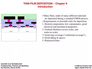
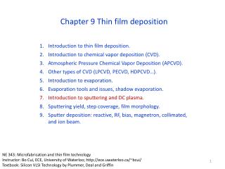
Chapter 9 Thin Film Deposition. Introduction. The layers on top of the silicon substrate are usually deposited Dielectrics Silicon oxide, silicon nitride Semiconductors poly-Si or a-Si Metals 95% Al/5% Si Ti or W clad copper Silicides (metal-silicon molecule) Carbon.

Chapter 9 Thin Film Deposition
E N D
Presentation Transcript
Introduction • The layers on top of the silicon substrate are usually deposited • Dielectrics • Silicon oxide, silicon nitride • Semiconductors • poly-Si or a-Si • Metals • 95% Al/5% Si • Ti or W clad copper • Silicides (metal-silicon molecule) • Carbon
Characteristics of Deposition Quality of deposition • Composition of the film • Contamination levels • Defect density • Pinholes, step coverage • Mechanical properties • Stress • Electrical properties • Conductivity • Optical properties • Reflectivity
Introduction Composition • May vary with deposition method and parameters • Composition control is very important when the material can have a range of compositions • Ratio of alloys and multilayer stacks of materials can change the chemical, electrical, optical, and mechanical properties of film. Contamination • Unwanted moisture, undesired metals, incorporation of oxygen and halogens
Introduction Defects • Pinholes and other structural defects must be minimized • often result from particles on the surface of the wafer
Introduction Other quality considerations • Films must be stable • Particularly if there are further thermal or chemical procedures to be carried out on the wafer. • They must adhere to the substrate • They must have minimum stress
Introduction • Uniformity of Thickness • The films must be uniform across the wafer and from wafer to wafer • Variations in thickness as in (b) can lead to high electrical resistance and localized heating • Can lead to cracking from thermal cycling and electromigration
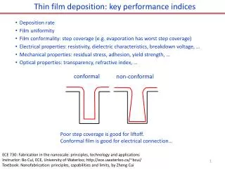
Step Coverage • Coverage of the side of the step • The ratio of the minimum thickness deposited on the side of the step divided by the thickness deposited on the top horizontal surface
Conformal step coverage • Refers to a step coverage of unity • Usually desired, but there are processes that rely on a step coverage of zero Conformal step coverage of PECVD SixNy http://www.hitech-projects.com/dts/docs/pecvd.htm
Aspect Ratio Deep, narrow features with high ARs are harder to fill PVD tantalum barrier layer with ~60% step coverage http://openlearn.open.ac.uk/mod/resource/view.php?id=257298
SEM image showing poor step coverage (breadloafing) of metal 1 into a silicon contact. (Courtesy Analytical Solutions) http://www.semitracks.com/reference/FA/die_level/sem/semxsc04.htm
Introduction • Space-filling properties • Via hole or contact hole filling with metal • Filling spaces or gaps in shallow trenches or between metal lines • Voids in the film itself or between film and semiconductor • High contact or sheet resistance • Voids can lead to cracking of dielectrics
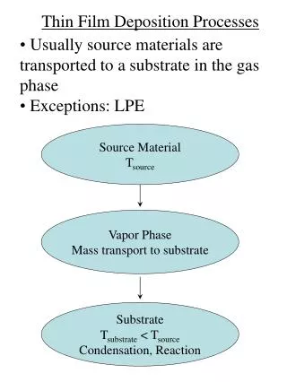
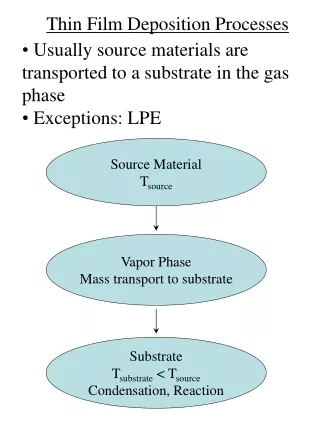
Two main categories of thin fim deposition • They are: • Chemical vapor deposition (CVD) • Physical vapor deposition (PVD) • Wafer is placed in a chamber and the constituents of the film are delivered in the gas phase to the surface where they form a film
Chemical Vapor Deposition • Reactant gases are introduced to the chamber • One or more than one gas may be used plus carrier gases (nonreactive gases) • In some cases, there is no gas source for a particular material so an inert carrier gas (Ar, N2) is bubbled bubble through a liquid source and the vapor is transported into the chamber.
Chemical Vapor Deposition • The system is designed so that the chemical reactions between the gases takes place on or very close to the wafer surface and not in the gas stream to produce the film • Particles produced in the gas stream rain down on the wafer surface and cause pinholes or low density films • CVD is used to deposit Si and dielectrics because of good quality films and good step coverage
Chemical Vapor Deposition • There are several variants of the process • Atmospheric pressure (APCVD) • Low pressure (LPCVD) • Plasma-enhanced (PECVD) • Most processes take place at elevated temperatures (250-650oC) • Increase reaction rate • Provide kinetic energy to allow reaction products to move along wafer surface • Increases film density and reduces pinholes and voids
A. Transport of Reactions to Wafer Surface in APCVD • Transport of reactants by forced convection to the deposition region • Transport of reactants by diffusion from the main gas stream to the wafer surface • Turbulent flow can produce thickness nonuniformities • Depletion of reactants can cause the film thickness to decrease in direction of gas flow • Adsorption of reactants on the wafer surface
APCVD B. Chemical reaction • Surface migration • Site incorporation on the surface • Desorption of byproducts • Removal of chemical byproducts • Transport of byproduct through the boundary layer • Transport of byproducts by forced convection away from the deposition region
Issues in APCVD • Release of the reactants or reaction product from the surface • Defined by the “sticking coefficient” • Composition of surface changes sticking coefficient • Re-emission is important in coverage and filling • Reaction on the chamber walls • cold wall versus hot wall processes • Wafer surface topology • surface diffusion of reactants and byproducts
Model for APCVD • Simple model for the two important processes • Mass transfer of reactants to wafer surface • Surface reactions • Equate these two steps under steady state conditions • The model looks very much like the model we developed for oxidation
APCVD • The problem can be set up as follows • There are two fluxes of atoms: F1 and F2
APCVD • Flux from the gas phase is driven by the concentration gradient from the flowing gas to Si surface through a stagnant boundary layer • Laminar flow condition • It is given (in molecules/cm2/s) byhG is the mass transfer coefficient through the boundary layer
APCVD • Flux that is consumed by the reaction at the surface is if the reaction is a first order reaction.kS is the chemical reaction rate at the surface (cm/s)
APCVD • At steady state – if two fluxes are equal • The growth rate of the film, v (cm/s), is • Where N is the number of atoms incorporated into the film per unit volume • For single composition film, this is the density
Mole fraction • The mole fraction in incorporating species in the gas phasewhere CT is the concentration of all molecules in the gas phase
Two limiting cases for APCVD model • Surface reaction controlled case (kS<<hG) • Mass transfer or gas-phase diffusion controlled case(hG<<kS)
APCVD • Both cases predict linear growth rates • but they have different coefficients • There is no parabolic growth rate • Surface reaction rate constant is controlled by Arrhenius-type equation (X=Xoe-E/kT) • Quite temperature sensitive • Mass transfer coefficient is relatively temperature independent • Sensitive to changes in partial pressures and total gas pressure
Epitaxial deposition of Si • Slopes of the reaction-limited graphs are all the same • activation energy of about 1.6 eV • This implies the reactions are similar; just the number of atoms is different • There is reason to believe that desorption of H2 from the surface is the rate limiting step • In practice • epitaxial Si at high temperatures (mass transfer regime) • poly-Si is deposited at low temperatures (reaction limited, low surface mobility)
Deposition of Si • Choice of gas affect the overall growth rate • Silane (SiH4) is fastest • SiCl4 is the slowest • Growth rate in the mass transfer regime is inversely dependent on the square root of the source gas molecular weight • Growth rate is dependent on the crystallographic orientation of the wafer • (111) surfaced grow slower than (100) • Results in faceting on nonplanar surfaces
APCVD • In the preceding theory, assumed hG and Cs were constants • Real systems are more complex than this • Consider the chamber where wafers lie on a susceptor (wafer holder). • Stagnant boundary layer, S, is not a constant, but varies along the length of the reactor • Cs varies with reaction chamber length as reaction depletes gases
Effects • Changes the effective cross section of the tube, which changes the gas flow rate • Increasing the flow rate reduces the thickness of the boundary layer and increases the mass transfer coefficient • Reduces gas diffusion length • To correct for the gas depletion effect, the reaction rate is increased along the length of the tube by imposing an increasing temperature gradient of about 5—25oC
APCVD • Sometimes we wish to dope the thin films as they are grown (e.g. PSG, BSG, BPSG, polysilicon, and epitaxial silicon). • Addition of dopants as gases for reaction • AsH3, B2H6, or PH3. • Surface reactions now include • Dissociation of the added doping gases • Lattice site incorporation of dopants • Coverage of dopant atoms by the other atoms in the film
APCVD • Another problem, common in CMOS production, is unintentional doping of lightly doped epitaxial Si when depositing them on a highly doped Si substrate. • Occurs by diffusion because of the high deposition temperatures (800—1000oC) • Growth rate of the deposited layers is usually much faster than diffusion rates (vt >> √Dt), the semi-infinite diffusion model can be applied
Mass transport on to deposited films • Atoms can outgas or be transported by carrier gas from the substrate into the gas stream and get re-deposited downstream • The process is called autodoping • Empirical expression to describe autodoping • C*S is an effective substrate surface concentration and L is an experimentally determined parameter • As film grows in thickness, dopant must diffuse through more film and less dopant enters gas phase.
Autodoping • Autodoping from the backside, edges, or other sources usually results in a relatively constant level. • This is because the source of dopant does not diminish as quickly but is at a much lower level.
APCVD The left part of the curve arises from the out-diffusion from the substrate The straight line part arises from the front-side autodiffusion The background (constant) part is from backside autodoping