Download
1 / 41
900 likes | 2.17k Vues
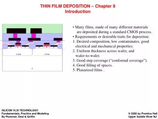
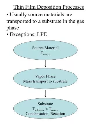
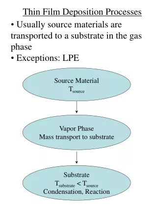
Chapter 9 Thin film deposition. Introduction to thin film deposition. Introduction to chemical vapor deposition (CVD). Atmospheric Pressure Chemical Vapor Deposition (APCVD). Other types of CVD (LPCVD, PECVD, HDPCVD…). Introduction to evaporation.

E N D
Chapter 9 Thin film deposition • Introduction to thin film deposition. • Introduction to chemical vapor deposition (CVD). • Atmospheric Pressure Chemical Vapor Deposition (APCVD). • Other types of CVD (LPCVD, PECVD, HDPCVD…). • Introduction to evaporation. • Evaporation tools and issues, shadow evaporation. • Introduction to sputtering and DC plasma. • Sputtering yield, step coverage, film morphology. • Sputter deposition: reactive, RF, bias, magnetron, collimated, and ion beam. NE 343: Microfabrication and thin film technology Instructor: Bo Cui, ECE, University of Waterloo; http://ece.uwaterloo.ca/~bcui/ Textbook: Silicon VLSI Technology by Plummer, Deal and Griffin
Sputter deposition Figure 9-2 Schematic diagram of DC-powered sputter deposition equipment. • Plasma is needed to make the gas conductive, and generated ions can then be accelerated to strike the target. • Higher pressures than evaporation: 1-100 mTorr. • Better at depositing alloys and compounds than evaporation. • The plasma contains ≈ equal numbers of positive argon ions and electrons as well as neutral argon atoms. Typically only <0.01% atoms are ionized!
Sputtering process • Sputtering process can be run in DC or RF mode (insulator must be run in RF mode) • Major process parameters: • Operation pressure (1-100mTorr) • Power (few 100W) • For DC sputtering, voltage -2 to -5kV. • Additional substrate bias voltage. • Substrate temperature (20-700oC) • In addition to IC industry, a wide range of industrial products use sputtering: LCD, computer hard drives, hard coatings for tools, metals on plastics. • It is more widely used for industry than evaporator, partly because that, for evaporation: • There are very few things (rate and substrate temperature) one can do to tailor film property. • The step coverage is poor. • It is not suitable for compound or alloy deposition. • Considerable materials are deposited on chamber walls and wasted. Targets for sputter deposition.
Sputter deposition advantages • Advantages: • Able to deposit a wide variety of metals, insulators, alloys and composites. • Replication of target composition in the deposited films. • Capable of in-situ cleaning prior to film deposition by reversing the potential on the electrodes . • Better film quality and step coverage than evaporation. • This is partly because adatoms are more energetic, and film is ‘densified’ by in-situ ion bombardment, and it is easier to heat up to high T than evaporation that is in vacuum. • More reproducible deposition control – same deposition rate for same process parameters (not true for evaporation), so easy film thickness control via time. • Can use large area targets for uniform thickness over large substrates. • Sufficient target material for many depositions. • No x-ray damage. • Disadvantages: • Substrate damage due to ion bombardment or UV generated by plasma. • Higher pressures 1 –100 mtorr ( < 10-5torr in evaporation), more contaminations unless using ultra clean gasses and ultra clean targets. • Deposition rate of some materials quite low. • Some materials (e.g., organics) degrade due to ionic bombardment. • Most of the energy incident on the target becomes heat, which must be removed.
Mechanisms of sputtering and alloy sputtering The ion impact may set up a series of collisions between atoms of the target, possibly leading to the ejection of some of these atoms. This ejection process is known as sputtering. Here we are interested in sputter deposition. Of course sputter can also be used as an etching method (the substrate to be etched will be the ‘target’), which is called sputter etching. Unlike evaporation, composition of alloy in film is approximately the same as target. Target NOT melted, slowdiffusion(no material flow) mixing. When target reaches steady state, surface composition balances sputter yield.
DC plasma Plasma is ionized gas, with nearly equal number of ions and electrons, plus neutrals (un-ionized molecules including those at ground state and excited state; free radicals such as atomic O, H, F – but no free radicals for Ar plasma). Glow is due to de-excitation of excited Ar. So glow only exists where there are lots of electrons to excite Ar. Cathode glow region: very close to cathode, secondary electrons are created by Ar bombardment of target material. Cathode dark space/sheath: electrons pass too fast with little excitation. Anode sheath: electrons lost to anode due to its faster random movement. e is decelerated (!!) toward anode Electron impact ionization
Explanation of DC plasma structure Different velocities in a plasma: Thermal energy random movement of Ar – 400 m/sec, order (kBT/mAr)1/2. Thermal energy random movement of electron – 10000 m/sec. Velocity of Ar with energy 100eV – 20000 m/sec. Velocity of electrons with energy 100eV – 6000000 m/sec. Thus plasma is highly conducting due to fast electrons – very little voltage drop in the plasma area where electrons are rich. Voltage drop is only possible near the electrodes where electrons may lost to the electrode. Even without applied voltage (assume plasma still exist), voltage drop may still exist due to faster random electrons movement that leads to their lost to electrode. Therefore, the plasma is always positively biased relative to any electrode or anything (floating or not) inside the plasma. This positive bias will accelerate positive Ar ion to strike the electrode. But the bias VP near the anode is very small (10V), so no significant sputtering of the substrate. The total bias (VP plus applied voltage) is very high, leading to sputtering of cathode (target).
Requirement for self-sustained discharge (plasma) Ions make (secondary) electrons when they bombard the target, and electrons make ions when they collide with Ar self sustained discharge. Condition for sustaining plasma: pd > 0.5 (cmTorr). For instance, typical target-substrate spacing d 10cm, need p > 50mTorr (actually sputter deposition is usually conducted at <10mTorr, due to magnetron… ). Condition for igniting the plasma. Too large Pd leads to too many collisions that prevent electron energy buildup. Too small Pd, there will be too few collisions (electron just goes to the wall without ionizing a molecule or atom), and too few ions to bombard and generate secondary electrons. Once the plasma is ignited, it is very conductive, thus voltage drops to order 100 V only.
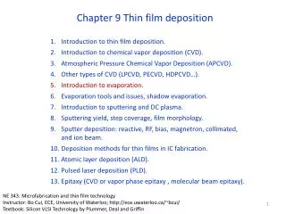
Chapter 9 Thin film deposition • Introduction to thin film deposition. • Introduction to chemical vapor deposition (CVD). • Atmospheric Pressure Chemical Vapor Deposition (APCVD). • Other types of CVD (LPCVD, PECVD, HDPCVD…). • Introduction to evaporation. • Evaporation tools and issues, shadow evaporation. • Introduction to sputtering and DC plasma. • Sputtering yield, step coverage, film property. • Sputter deposition: reactive, RF, bias, magnetron, collimated, and ion beam. NE 343: Microfabrication and Thin Film Technology Instructor: Bo Cui, ECE, University of Waterloo, bcui@uwaterloo.ca Textbook: Silicon VLSI Technology by Plummer, Deal, Griffin
Sputtering process Figure 9-24 On the left side, sputter off an Al atom. On the right side, generate secondary electrons, which are accelerated across the sheath region and 1) ionize/excite an Ar; or 2) ionize an impurity atom, here O, to generate O- (for Ar, always positive ion Ar+). This O- is accelerated toward substrate and may go into the film (bad). After collision ionization, there are now TWO free electrons. This doubles the available electrons for ionization. This ongoing doubling process is called "impact ionization”, which sustains a plasma.
Sputtering process • Energy of each incoming ion is 500-1000eV.Energy of sputtered atoms is 3-10eV. • Thus, the sputtering process is very inefficient from the energy point of view,95% ofincoming energy goes to target heating & secondary electron. • High rate sputter processes need efficient cooling techniques to avoid target damage from overheating (serious problem). • The sputtered species, in general, are predominantly neutral. • The energy of the ejected atoms shows a Maxwellian distribution with a long tail toward higher energies. • The energies of the atoms or molecules sputtered at a given rate are about one order of magnitude higher than those thermally evaporated at the same rate, which often lead to better film quality. • However, since sputtering yields are low and the ion currents are limited, sputter-deposition rates are invariably one to two orders of magnitude lower compared to thermal evaporation rates under normal conditions.
Sputtering yield Elastic energy transfer E2 is greatest for M1=M2. There is also inelastic energy transfer, which leads to secondary electrons emission… • Sputter yield Y: the number of sputtered atoms per impinging ion. • Obviously, the higher yield, the higher sputter deposition rate. • Sputter yield is 1-3: not too much difference for different materials. • The sputter yield depends on: (a) the energy of the incident ions; (b) the masses of the ions and target atoms; (c) the binding energy of atoms in the solid; and (d) the incident angle of ions. • The yield is rather insensitive to the target temperature except at very high temperatures where it show an apparent rapid increase due to the accompanying thermal evaporation.
Dependence of sputter yield on ion energy A threshold energy for the release of an atom from the target exists, below which the atom is not “sputtered”. This threshold energy is: The yield increases with the energy. For higher energies, the yield approaches saturation, which occurs at higher energies for heavier bombarding particles. e.g.: Xe+100keV and Ar+20KeV for saturation. Sometimes, at very high energies, the yield decreases because of the increasing penetration depth and hence increasing energy loss below the surface, i.e. not all the affected atoms are able to reach the surface to escape. (Eth very high when M1M2 or they are very different?)
Dependence of sputter yield on ion energy (log scale) (keV)
Dependence of sputter yield on ion incident angle The yield increases as (cos)-1 with increasing obliqueness () of the incident ions. However, at large angles of incidence the surface penetration effect decrease the yield drastically. 60o – 70o Why Au is different? (rough)
Dependence of sputter yield on ion mass Sputter increases with ion mass. Sputter yield is a maximum for ions with full valence shells: noble gasses such as Ar, Kr, Xe have large yields. Sputter rate for Ag is higher than Cu, and Cu higher than Ta Ar
Dependence of deposition rate on chamber pressure Higher chamber pressure: Mean-free path of an atom =4.810-3/P(torr) (cm). E.g. 0.1cm for P=50mTorr. Therefore, as typically target-substrate separation is many cm, sputtered atoms have to go through tens of collisions before reaching the substrate. This reduces deposition rate – considerable materials are deposited onto chamber walls. Too many collisions also prevent ionization (reduce ion density and deposition rate). Lower chamber pressure: (For same power) higher ion energy that increases sputter yield/deposition rate. But fewer Ar ions to bombard the target for deposition, which reduces deposition rate. Therefore, there exist an optimum pressure (provided that such a pressure can sustain the plasma) for maximum deposition rate. This optimum pressure depends on target-substrate configurations (their separation, target/substrate size…).
Dependence of deposition rate on chamber pressure Too few collisions limit yield Too many collisions prevent ionization Figure 3-18 Influence of working pressure and current on deposition rate for non-magnetron sputtering. Plasma not sustained at low pressure Arcing in plasma (?) For same power P=IV=constant, high current (ion number) comes with low voltage (ion energy)
Step coverage of sputtering Sputtering targets are generally large and provide a wide range of arrival angles in contrast to a point source. Step coverage is mainly determined by arrival angle distribution. Figure 9-26 Small soure, wide emitted angle distribution, but a narrow arrival angle distribution. Wider arrival angle distriubtion. Arrival angle distribution is defined by arrival flux relative to unit surface area. The flux is equal to the normal component of incoming flux. Figure 9-25 Arrival angle distribution is generally described by cosn distribution. Size of source, system geometry and collisions in gas phase are important in arrival angle distribution.
Arrival angle can be tailored to some degree Standard sputtering. Long-throw sputtering. Sputtering with a collimator. However, when the mean free path of the target atom (determined by gas pressure, order 10cm for 1mTorr pressure/1cm for 10mTorr) is much shorter than target-substrate separation, many collisions will occur, which broaden the arrival angle distribution. More deposition on top surface.
Adatom migration along surface also important • Atoms ejected from cathode escape with energies of 10 to 50 eV, which is 10-100 times the energy of evaporated atoms. • This additional energy (together with bombardment by other ions) provides sputtered atoms with additional surface mobility for improved step coverage relative to evaporation. • (This additional energy also makes the deposited film “denser” - better film quality than evaporated film). • Besides tilting and rotating substrate, step coverage can be further improved by: • Substrate heating: improve step coverage due to surface diffusion, but may produce unacceptably large grains. • Apply bias to wafers: increase bombardment by energetic ions, but it will also sputter the deposited material off the film and thus reduce deposition rate.
Film morphology: the zone model Zone model: film morphology as a function of substrate temperature and incident ion energy. Once reach wafer surface, adatoms (newly added atom) diffuse along surface until they form nuclei. Nuclei capture more adatoms, forming islands. If surface mobility is high, islands may merge, forming a smooth continuous film. Zone 1: porous and/or amorphous due to poor surface mobility, which is in-turn caused by low temperature and/or low ion energy (due to low RF power/DC bias or higher pressures - less acceleration between collisions). Metal films in this region can readily oxidize when exposed to air and so may have high resistivity. Zone model of film deposition. Tm: melting temperature. Zone 2 (“T-zone”): most desirable, small grain polycrystalline, dense, smooth (high reflectance) due to higher surface mobility (higher temperature and/or ion energy). Zone 3: further increases in surface mobility result in large columnar grains that have rough surfaces. These rough surfaces lead to poor coverage in later steps. Zone 4: still further increases in surface mobility result in large non-columnar grains. These grains can pose problems for lithography due to light scatter off of large grains, and tend to be more rigid leading to more failures in electrical lines.
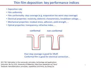
Chapter 9 Thin film deposition • Introduction to thin film deposition. • Introduction to chemical vapor deposition (CVD). • Atmospheric Pressure Chemical Vapor Deposition (APCVD). • Other types of CVD (LPCVD, PECVD, HDPCVD…). • Introduction to evaporation. • Evaporation tools and issues, shadow evaporation. • Introduction to sputtering and DC plasma. • Sputtering yield, step coverage, film morhology. • Sputter deposition: reactive, RF, bias, magnetron, collimated, and ion beam. NE 343: Microfabrication and Thin Film Technology Instructor: Bo Cui, ECE, University of Waterloo, bcui@uwaterloo.ca Textbook: Silicon VLSI Technology by Plummer, Deal, Griffin
Reactive sputtering Sputtering metallic target in the presence of a reactive gas mixed with inert gas (Ar). • Sputtering a compound target may not give what one wants. • This doesn’t mean reactive sputtering will give what one wants – it is just one more thing to try with. • Certainly reactive sputtering can be done using DC sputtering, whereas compound target (insulating) can only be used for RF sputtering. • Chemical reaction takes place on substrate and target. • Can “poison” target if chemical reactions are faster than sputter rate. • Need to adjust reactive gas flow to get good composition (e.g. SiO2 rather than SiO2-x) without incorporating excess gas into film. A mixture of inert + reactive gases used for sputtering: Oxides – Al2O3, SiO2, Ta2O5 (O2 mixed with Ar) Nitrides – TaN, TiN, Si3N4 (N2, NH3, mixed with Ar) Carbides – TiC, WC, SiC (CH4, C2H4, C3H8, mixed with Ar)
RF (radio frequency) sputter deposition • Good for insulating materials because, positive charge (Ar+) build up on the cathode (target) in DC sputtering systems. Alternating potential can avoid charge buildup • When frequencies less than 50kHz, both electrons and ions can follow the switching of the anode and cathode, basically DC sputtering of both surfaces. • When frequencies well above 50kHz, ions (heavy) can no longer follow the switching, and electrons can neutralize positive charge buildup on each electrode during each half cycle. • As now electrons gain energy directly from RF powder (no need of secondary electrons to maintain plasma), and oscillating electrons are more efficient to ionize the gas, RF sputter is capable of running in lower pressure (1-15 mTorr), so fewer gas collisions and more line of sight deposition. 13.56MHz RF source Switch polarities before the target surface saturates with ions.
RF plasma • For symmetric target-substrate configuration, sputtering of both surfaces will occur, though in the opposite half cycles. • When the electrode areas are not equal, the field must be higher at the smaller electrode (higher current density), to maintain overall current continuity. • It was found that voltage drop across the dark sheath of the two electrodes satisfy the relation: (A is the area of the electrode) • Thus by making the target electrode much smaller, sputtering occurs "only" on the target. • Wafer electrode can also be connected to chamber walls, further increasing V2/V1. (m = 1-2 experimentally) Figure 9-27
Bias sputter deposition (small negative bias at wafer chuck) • Wafer chuck no longer connected to chamber wall, so one can apply a negative DC or RF bias (self generated bias across the sheath region) relative to chamber wall. • More bombardment/etch of substrate, but deposition rate is faster than etching rate. • Obviously the net deposition rate is lower than regular (without bias) sputter deposition. • Increased bombardment of film may improve film quality. • Can be used for wafer cleaning before deposition, or used to improve step coverage. • One mechanism for improved step coverage is re-deposition of sputtered materials onto vertical sidewalls (see figure below). One mechanism for improved step coverage is re-deposition of sputtered film material.
Bias sputter deposition to improve step coverage: a second mechanism 60o – 70o Sputtered away material Figure 9-29 Illustration of angle-dependent sputtering which removes non-planar features in bias-sputter deposition. Here the angled surfaces of the overhang are preferentially sputtered by the directed ions, allowing for better filling of the hole. Note that sputter rate is lowest for vertical (90o ion incident angle) and horizontal surfaces (0o ion incident angle).
Magnetron sputtering • In DC & RF sputtering, the efficiency of ionization from energetic collisions between the electrons and gas atoms is low. • Most electrons lose energy in non-ionizing collisions or are collected by the electrodes. • Oscillating RF fields increasing ionization efficiency marginally. • Hence, deposition rates are low. • To increase deposition rates, magnets are used to increase the percentage of electrons that take part in ionization events, increasing the ionization efficiency. • A magnetic field is applied at right angles to the electric field by placing large magnets behind the target. • This traps electrons near the target surface and causes them to move in a spiral motion until they collide with an Ar atom. • The ionization and sputtering efficiencies are increased significantly - deposition rates increase by 10-100, to 1 m per minute. • Unintentional wafer heating is reduced since the dense plasma is confined near the target and ion loss to the wafers is less. • A lower Ar pressure (to 0.5mTorr, can still sustain plasma) can be utilized since ionization efficiency is larger which can improve film quality as less argon will be incorporated into the film. • Magnetron sputtering can be done in DC or RF, but more often it is done in DC as cooling of insulating targets is difficult in RF systems.
Magnetron sputtering Orbital motion of electrons increases probability that they will collide with neutral species and create ions. Magnetron sputtering for high density of plasma near target.
Impact of magnetic field on ions Hoping radius r: Vd: voltage drop across dark space/sheath (100V) B: magnetic field (100G) For electron: r0.3cm For Ar+ ion: r81cm • As a result: • Current density (proportional to ionization rate) increases by 100 times. • Required discharge pressure drops 100 times. • Deposition rate increases 100 times. (non-magnetron can work at 10mTorr)
Magnetron sputtering For some applications (e.g. filling of high aspect ratio holes), small target and large target-substrate separation is used, in order to achieve narrow arrival angle distribution. (long throw sputtering) This is possible only if the atoms don’t experience many collisions on their path to the substrate. This means a large mean free path and a low chamber pressure, which can be achieved using magnetron sputtering. E.g., 10cm mean free path for 0.5mTorr pressure (but this value is for Ar, not the material to be deposited). When the pressure is not that low, most atoms will be deposited onto chamber wall. (Those reaching the substrate still have narrow arrival angle distribution) A magnetron sputter gun, magnet under target (not seen) Issues for magnetron sputtering: Erosion track in the target, leading to poor target use efficiency and non-uniform film on substrate.
Collimated sputtering The goal is to fill high aspect ratio holes by more directional sputtering with narrow arrival angle distribution. The long throw sputtering (previous slide) is one kind of “collimated” sputtering, but also with low efficiency. Collimated sputtering • Insert a plate with high-aspect-ratio holes. • Sputter at low pressure, mean path is long enough that few collisions occur between collimator and wafer. • Species with velocities nearly perpendicular to wafer surface pass through the holes. • Reduce deposition rate considerably (most sputtered atoms cannot reach the substrate).
Ionized sputter deposition • The depositing atoms themselves are ionized. • An RF coil around the plasma induces collisions in the plasma, creating the ions (50-85% ionized). • Most sputtered atoms can reach the substrate, thus it is a better solution than a collimator. • This, again, provides a narrow distribution of arrival angles, which may be useful when filling or coating the bottom of deep contact hole. Figure 9-31 Figure 9-30 Regular sputter deposition. Collimated sputter deposition, by using long throw configuration, a collimator, or ionized sputter deposition.
Ion beam sputter deposition (IBSD) • High-end thin film deposition process. • Lower pressure sputter deposition (10-4Torr), sputtered atoms retain kinetic energy due to minimal scatting in low pressure environments. • High quality, smooth, pin hole free films. • Enhanced adhesion and micro-structure control. • Yields excellent coverage at small thicknesses and on high aspect ratio features. • Independent control of ion beam parameters allows user to engineer film for desired properties. • Low energy ion source (left) assists with end-hall ion source (right). • Typically, film properties from ion beam deposition exceed those deposited by evaporation or magnetron sputtering. Typical ion beam sputter deposition system, with ion beam assisted deposition capability for cluster tool configuration
Comparison of evaporation and sputtering Evaporation Sputtering