Digital Electronics
Digital Electronics. Lecture 7 Sequential Logic Circuit Design. Announcements. http://www.uobkupartnership.talktalk.net Books, CD Exam and further teaching of electronics Digital Systems, Principles and Applications, 10th Edition R.J Tocci, N. S. Windmer , G. L. Moss, 2007.

Digital Electronics
E N D
Presentation Transcript
Digital Electronics Lecture 7 Sequential Logic Circuit Design
Announcements http://www.uobkupartnership.talktalk.net Books, CD Exam and further teaching of electronics • Digital Systems, Principles and Applications, 10th Edition • R.J Tocci, N. S. Windmer, G. L. Moss, 2007. • Kleitz, W., Digital Electronics, Pearson Education Inc, 2005. • Clements, A, Microproscessor System Design, PWS-Kent publishing Copany, 1992.
Lecture 6 outline • Review of last Lecture • Sequential Logic Circuits • Basic Latch • Flip-Flops
Review of Last Lecture • Design procedure for combinational logic circuits. • Adders • Multiplexer • Simulation exercises using logic converter
Sequential Logic Circuits • Any sequential logic system can be broken down into two sections: • Memory part • combinational part • The combinational part will comprise the usual AND, OR gates etc. • The memory part is usually implemented with bistable devices. • Two basic types: latches and flip-flops.
Sequential Logic Circuits • Any sequential logic system can be broken down into two sections: • Memory part • combinational part • The combinational part will comprise the usual AND, OR gates etc. • The memory part is usually implemented with bistable devices. • Two basic types: latches and flip-flops.
A latch changes state when the input states change. This property is known as transparency. Data is stored by the latch when an enable input (if provided) is valid. • A flip-flop however can only change state on the application of a clock pulse. • A purely sequential system is one in which the output is determined by the order in which the input signals are applied. • Sequential circuits are classified as asynchronous (unclocked) or synchronous (clocked).
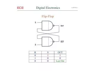
The Basic Latch • The basic latch has two stable states that correspond to a logic 1 and logic 0. The output changes from one state to another depending on the inputs. • Consider the simple latch shown below. Truth table as shown below:
This is the basis of the SR (or RS) latch , where A=R, B=S, X=Q and Y=/Q. The circuit symbol is shown below. This is the basis of the SR (or RS) latch , where A=R, B=S, X=Q and Y=/Q. The circuit symbol is shown below.
The Gated SR Latch The inputs to a gated Latch are controlled by a gate/enable/clock input which allows the latch inputs A and B to be active only when a logic 1 is present on the clock input. This therefore is a level activated device. The Gated SR Latch The truth table is now: The function of the RS gated latch can be illustrated with a waveform diagram as shown below.
The truth table is now: • The truth table is now: • Symbol The function of the RS gated latch can be illustrated with a waveform diagram as shown below.
The JK Flip-Flop • The JK flip-flop is basically an SR gated latch with modifications to eliminate the problems of the final indeterminate state. When the two inputs J and K are both 1 then the output Q changes state. It is said to toggle under these conditions. • Circuit Symbol:
Truth table Truth table:
Excitation table Truth table:
The D-Type Flip-Flop • The D (data) type flip-flop is basically a single-bit storage device. It can be constructed by connecting an inverter between the J and K inputs of a JK flip-flop as shown overleaf.
Data appearing on the data input D is simply clocked through to the output Q on the application of a clock pulse. • Symbol:
The T-Type Flip-Flop • The T (toggle) type flip-flop also has a single input. It too can be implemented using a JK flip-flop; the inputs are simply connected together as shown below
PR ESET and Clear inputs • Positive and negative edged triggered devices
Main Points • Sequential Logic Circuits. • Latch • J-K flip-flop • D – Type flip-flop • T-type flip-flop • Counters • Shift register
The End • Thank you for your attention.