
Uploaded by
acacia
1 SLIDES
140 VUES
10LIKES
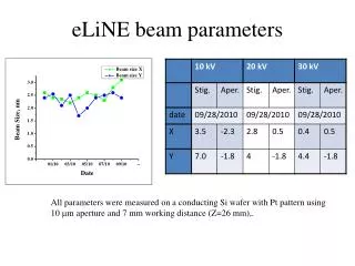
eLiNE beam parameters
DESCRIPTION
This study details the measurement parameters obtained from a conductive silicon wafer featuring a platinum pattern. Utilizing a 10 mm aperture and a working distance of 7 mm, with Z positioned at 26 mm, precise metrics were gathered to analyze the conductivity and structural properties. The findings can provide insights into semiconductor behavior and the impact of patterning on electrical performance. This comprehensive evaluation allows for further development in microfabrication techniques and applications in electronic devices.
Download
1 / 1
Télécharger la présentation 
eLiNE beam parameters
An Image/Link below is provided (as is) to download presentation
Download Policy: Content on the Website is provided to you AS IS for your information and personal use and may not be sold / licensed / shared on other websites without getting consent from its author.
Content is provided to you AS IS for your information and personal use only.
Download presentation by click this link.
While downloading, if for some reason you are not able to download a presentation, the publisher may have deleted the file from their server.
During download, if you can't get a presentation, the file might be deleted by the publisher.
E N D
Presentation Transcript
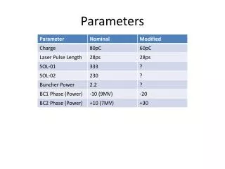
eLiNE beam parameters All parameters were measured on a conducting Si wafer with Pt pattern using 10 mm aperture and 7 mm working distance (Z=26 mm),.


More Related