Download
1 / 2
20 likes | 190 Vues
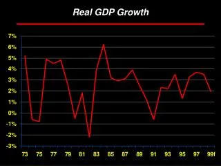
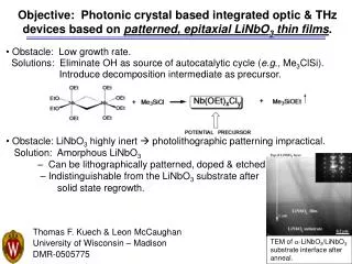
TEM of a -LiNbO 3 /LiNbO 3 substrate interface after anneal. Objective: Photonic crystal based integrated optic & THz devices based on patterned, epitaxial LiNbO 3 thin films. Obstacle: Low growth rate. Solutions: Eliminate OH as source of autocatalytic cycle ( e.g ., Me 3 ClSi).

E N D
TEM of a-LiNbO3/LiNbO3 substrate interface after anneal. Objective: Photonic crystal based integrated optic & THz devices based on patterned, epitaxial LiNbO3 thin films. • Obstacle: Low growth rate. • Solutions: Eliminate OH as source of autocatalytic cycle (e.g., Me3ClSi). • Introduce decomposition intermediate as precursor. • Obstacle: LiNbO3 highly inert photolithographic patterning impractical. • Solution: Amorphous LiNbO3 • – Can be lithographically patterned, doped & etched. • – Indistinguishable from the LiNbO3 substrate after • solid state regrowth. Thomas F. Kuech & Leon McCaughan University of Wisconsin – Madison DMR-0505775
Results: Growth rate doubles with Me3SiCl as a Reactive Carrier Gas. Intermediate Nb(OEt)xCly as a precursor. Amorphous LiNbO3 (or Ti:LiNbO3) film easily patterned by standard photolithography and wet etching. Objective: Photonic crystal based integrated optic & THz devices based on patterned, epitaxial LiNbO3 thin films. RIE: THz photonic crystal (a~ 7 mm) FIB: IR photonic crystal (a~2 mm) Payoff: Enable a new class of truly compact, ultra-fast electro-optic and all-optical devices and circuits. • Outreach efforts focus on the inclusion of undergraduate women in the program research Ridge Waveguides Thomas F. Kuech & Leon McCaughan University of Wisconsin – Madison DMR-0505775