Combinational Logic
Combinational Logic. Mantıksal Tasarım – BBM231 M. Önder Efe onderefe@cs.hacettepe.edu.tr. Classification. Combinational no memory outputs depends on only the present inputs expressed by Boolean functions Sequential storage elements + logic gates

Combinational Logic
E N D
Presentation Transcript
Combinational Logic Mantıksal Tasarım – BBM231 M. Önder Efe onderefe@cs.hacettepe.edu.tr
Classification • Combinational • no memory • outputs depends on only the present inputs • expressed by Boolean functions • Sequential • storage elements + logic gates • the content of the storage elements define the state of the circuit • outputs are functions of both input and current state • state is a function of previous inputs • outputs not only depend the present inputs but also the past inputs
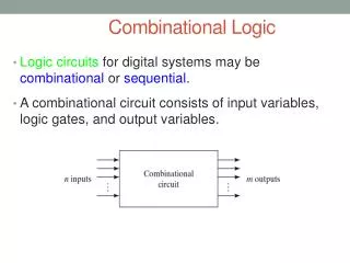
Combinational circuit (logic gates) n binary inputs m binary outputs Combinational Circuits • n input bits 2n possible binary input combinations • For each possible input combination, there is one possible output value • truth table • Boolean functions (with n input variables) • Examples: adders, subtractors, comparators, decoders, encoders, and multiplexers.
Analysis & Design of Combinational Logic • Analysis: to find out the function that a given circuit implements • We are given a logic circuit and • we are expected to find out • Boolean function(s) • truth table • A possible explanation of the circuit operation (i.e. what it does) • Firstly, make sure that the given circuit is, indeed, combinational.
Analysis of Combinational Logic • Verifying the circuit is combinational • No memory elements • No feedback paths (connections) • Secondly, obtain a Boolean function for each output or the truth table • Lastly, interpret the operation of the circuit from the derived Boolean functions or truth table • What is it the circuit doing? • Addition, subtraction, multiplication, etc.
a F1 b c a b c a b F2 a c b c Obtaining Boolean Function Example T1 T2 T4 T3
Example: Obtaining Boolean Function • Boolean expressions for named wires • T1 = abc • T2 = a + b + c • F2 = ab + ac + bc • T3 = F2’ = (ab + ac + bc)’ • T4 = T3T2 = (ab + ac + bc)’ (a + b + c) • F1 = T1 + T4 = abc + (ab + ac + bc)’ (a + b + c) = abc + ((a’ + b’)(a’ + c’)(b’ + c’)) (a + b + c) = abc + ((a’ + a’c’ + a’b’ + b’c’)(b’ + c’)) (a + b + c) = abc + (a’b’ + a’c’ + a’b’c’ + b’c’)(a+b+c)
Example: Obtaining Boolean Function • Boolean expressions for outputs • F2 = ab + ac + bc • F1 = abc + (a’b’ + a’c’ + b’c’) (a + b + c) • F1 = abc + a’b’c + a’bc’ + ab’c’ • F1 = a(bc + b’c’) + a’(b’c + bc’) • F1 = a(b c)’ + a’(b c) • F1 =
Example: Obtaining Truth Table • F1 = • F2 = ab + ac + bc carry sum This is what we call full-adder (FA)
Design of Combinational Logic • Design Procedure: • We start with the verbal specification about what the resulting circuit will do for us (i.e. which function it will implement) • Specifications are often verbal, and very likely incomplete and ambiguous (if not faulty) • Wrong interpretations can result in incorrect circuit • We are expected to find • firstly, Boolean function(s) (or truth table) to realize the desired functionality • Logic circuit implementing the Boolean function(s) (or the truth table)
Possible Design Steps • Find out the number of inputs and outputs • Derive the truth table that defines the required relationship between inputs and outputs • Obtain asimplified Boolean function for each output • Draw the logic diagram (enter your design into CAD) • Verify the correctness of the design
Design Constraints • From the truth table, we can obtain a variety of simplified expressions • Question: which one to choose? • The design constraints may help in the selection process • Constraints: • number of gates • propagation time of the signal all the way from the inputs to the outputs • number of inputs to a gate • number of interconnections • power consumption • driving capability of each gate
Example: Design Process • BCD-to-2421 Converter • Verbal specification: • Given a BCD digit (i.e. {0, 1, …, 9}), the circuit computes 2421 code equivalent of the decimal number • Step 1: how many inputs and how many outputs? • four inputs and four outputs • Step 2: • Obtain the truth table • 0000 0000 • 1001 1111 • etc.
BCD-to-2421 Converter • Truth Table
BCD-to-2421 Converter CD AB 00 01 11 10 00 0 0 0 0 01 0 1 1 1 11 10 1 1 • Step 3: Obtain simplified Boolean expression for each output • Output x: x = BD +BC + A
Output y: Boolean Expressions for Outputs • Output z:
Boolean Expressions for Outputs • Output t: • Step 4: Draw the logic diagram t = D x = BC + BD + A y = A + BD’ + BC z = A + B’C + BC’D
Example: Logic Diagram A B x = BC + BD + A C D y = A + BD’ + BC z = A + B’C + BC’D t = D
Example: Verification • Step 5: Check the functional correctness of the logic circuit • Apply all possible input combinations • And check if the circuit generates the correct outputs for each input combinations • For large circuits with many input combinations, this may not be feasible. • Statistical techniques may be used to verify the correctness of large circuits with many input combinations
Binary Adder/Subtractor • (Arithmetic) Addition of two binary digits • 0 + 0 = 0, 0 + 1 = 1, 1 + 0 = 1, and 1 + 1 = 10 • The result has two components • the sum (S) • the carry (C) • (Arithmetic) Addition of three binary digits
x S y C Half Adder • Truth table S = x’y + xy’ = x y C = xy HA HA
Full Adder 1/2 • A circuit that performs the arithmetic sum of three bits • Three inputs • the range of output is [0, 3] • Two binary outputs
Full Adder 2/2 • Karnaugh Maps S = xy’z’ + x’y’z + xyz + x’yz’ = ... = ... = x y z C = xy + xz + yz Two level implementation 1st level: three AND gates 2nd level: One OR gate
x HA S HA S y C C C z Full Adder: Hierarchical Realization • Sum • S = x y z • Carry • C = xy + xz + yz = (x + y) z + xy = (x y) z + xy • This allows us to implement a full-adder using two half adders. x y z = S
HA HA x y S C z Full Adder Using Half Adders
a0 b0 a1 b1 a2 b2 a3 b3 HA y FA x FA y y FA y x x x C1 C2 C3 C4 C z z z C C C S S S S S0 S1 S2 S3 Integer Addition 1/2 • Binary adder: • A digital circuit that produces the arithmetic sum of two binary numbers • A = (an-1, an-2, …, a1, a0) • B = (bn-1, bn-2, …, b1, b0) • A simple case: 4-bit binary adder
Integer Addition 2/2 a0 b0 a1 b1 a2 b2 a3 b3 FA y FA x FA y y FA y x x x C0=0 C1 C2 C3 C4 z C z z z C C C S S S S S0 S1 S2 S3 Ripple-carry adder
Hierarchical Design Methodology • The design methodology we used to build carry-ripple adder is what is referred as hierarchical design. • In classical design, we have: • 9 inputs including C0. • 5 outputs • Truth tables with 29 = 512 entries • We have to optimize five Boolean functions with 9 variables each. • Hierarchical design • we divide our design into smaller functional blocks • connect functional units to produce the big functionality
Recall how we do subtraction (2’s complement) X – Y = X + (2n – Y) = X + ~Y + 1 x0 y0 x2 x1 y1 x3 y3 y2 logic-1 4-bit adder circuit a3 b3 a2 b2 a1 b1 a0 b0 C4 C0 S3 S0 S1 S2 S3 S0 S1 S2 C4 Subtractor
CarryPropagation a0 b0 a1 b1 a2 b2 a3 b3 FA y FA x FA y y FA y x x x C0=0 C1 C2 C3 C4 z C z z z C C C S S S S S0 S1 S2 S3 Ripple-carry adder • What is the total propagation time of 4-bit ripple-carry adder? • FA: propagation time of a single full adder. • We have four full adders connected in cascaded fashion • Total propagation time: ??
ai bi Si Ci+1 Ci Carry Propagation • Propagation time of a fulladder • XOR 2AND= 2OR • FA 2XOR Pi Gi
Carry Propagation a0 a3 a2 a1 b3 b1 b2 b0 C0 P0 P1 C1 P2 C2 P3 C3 C1 C3 C2 C4 S1 S3 S2 S0 • Delays • P0, P1, P2, P3: XOR 2AND • C1(S0): 2AND + 2AND 4AND • C2(S1): 4AND + 2AND 6AND • C3(S2): 6AND + 2AND 8AND • C4(S3): 8AND + 2AND 10AND
a3 Carry Lookahead circuit P3 C4 C4 b3 G3 P3 S3 C3 a2 P2 b2 G2 P2 S2 C2 a1 P1 b1 P1 G2 S1 C1 a0 P0 b0 G0 P0 S0 C0 C0 4-bit Carry Lookahead Adder C0
2x4 decoder d0 x d1 d2 y d3 • d0 = • d1 = • d2 = • d3 = Decoders • A binary code of n bits • capable of representing 2n distinct elements of coded information • A decoder is a combinational circuit that converts binary information from n binary inputs to a maximum of 2n unique output lines
Decoder with Enable Input 2x4 decoder d0 x d1 d2 y d3 e
d0 2x4 decoder d0 x d1 d1 e d2 d2 d3 y d3 x, y e Demultiplexer • A demultiplexer is a combinational circuit • it receives information from a single inputline and directs it one of 2n output lines • It has n selection lines as to which output will get the input d0 = e when x = 0 and y = 0 d1 = e when x = 0 and y = 1 d2 = e when x = 1 and y = 0 d3 = e when x = 1 and y = 1
Demultiplexer 0 1 0 e 1 0 1 x1 x0
Demultiplexer 0 1 0 0 e 1 1 0 0 1 0 1 1 0 1 x2 x1 x0
Demultiplexer 0 1 0 1 0 1 0 1 x0
d0 2x4 decoder y d1 d2 z e d3 d4 2x4 decoder d5 d6 e d7 Combining Decoders x
Combining Decoders d0 nx2n Decoder-1 x0 d1 xn-1 e d2n-1 nx2n Decoder-2 e nx2n Decoder-2p e d2n+p-1-1 px2p Decoder xn xn+p-1
2x4 decoder d0 = x’y’ x d1 = x’y d2 = xy’ y d3 = xy Decoder as a Building Block • A decoder provides the 2n minterms of n input variable • We can use a decoder and OR gates to realize any Boolean function expressed as sum of minterms • Any circuit with n inputs and m outputs can be realized using an n-to-2n decoder and m OR gates.
d0 = x’y’z’ d4= xy’z’ d1 = x’y’z d5= xy’z d2 = x’yz’ d6= xyz’ d3 = x’yz d7= xyz Decoder as a Building Block-ROM 2x4 decoder x y z F2 F1 F0
Decoder as a Building Block-ROM 2x4 decoder x y z F2 F1 F0
0 3x8 decoder x 1 2 3 y 4 5 S 6 z 7 Example: Decoder as a Building Block • Full adder • C = xy + xz + yz • S = x y z C
Encoders • An encoder is a combinational circuit that performs the inverse operation of a decoder • number of inputs: 2n • number of outputs: n • the output lines generate the binary code corresponding to the input value • Example: n = 2
d0 d1 d2 d3 x y V 0 0 0 0 X X 0 1 0 0 0 0 0 1 X 1 0 0 0 1 1 X X 1 0 1 0 1 X X X 1 1 1 1 Priority Encoder • Problem with a regular encoder: • only one input can be active at any given time • the output is undefined for the case when more than one input is active simultaneously. • Priority encoder: • there is a priority among the inputs
4-bit Priority Encoder • In the truth table • X for input variables represents both 0 and 1. • Good for condensing the truth table • Example: X100 (0100, 1100) • This means d1 has priority over d0 • d3 has the highest priority • d2 has the next • d0 has the lowest priority • V = ?

