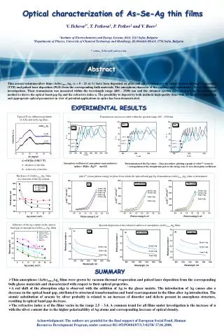
Download
1 / 11
110 likes | 320 Vues
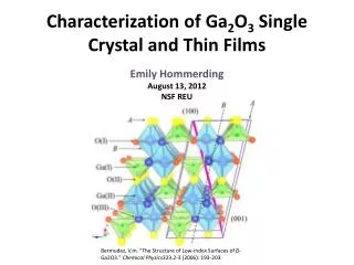
Characterization of CuInSe 2 Thin Films for Photovoltaics. Celina S. Dozier FAMU-FSU: Dr. Eric Kalu CMU: Dr. Paul Salvador. ZnO. CuInSe 2. e - Collecting Plate Ni. Substrate. Background. What is Photovoltaics? Process of converting sunlight into electricity

E N D
Characterization of CuInSe2 Thin Films for Photovoltaics Celina S. Dozier FAMU-FSU: Dr. Eric Kalu CMU: Dr. Paul Salvador
ZnO CuInSe2 e- Collecting Plate Ni Substrate Background • What is Photovoltaics? • Process of converting sunlight into electricity • A potential energy barrier that separate electrons and holes that are created by the absorption of sunlight • Creates a current
Semiconducting Materials • Qualities of a good PV material: • Strong light absorption • Low cost • Stability as functions of both time and illumination conditions • High abundance of source materials • Environmentally friendly technology
Copper Indium Diselenide • Conversion efficiencies of 17.8% have been reached for vapor-deposited CIS cells • The chalcopyrite structure of ternary I-III-VI2 compounds have high absorption coefficients making CIS well-suited for solar cells • Bandgap of 1.02 eV
Experiment • Production Procedure • Nickel is plated on Kapton/Mylar • A three-electrode setup used to deposit CIS • CIS was electrochemically deposited at the following potentials for 5 minutes: -0.35V, -0.55V, -0.75V, -1.0V, -1.1V • How does varying the deposition potential affect the lattice structure of CIS and surface morphology?
AFM Results 20 µm 20 µm Potential: -0.35 V Unannealed RMS Roughness: 654Å Grayscale: 0.5 µm Potential: -0.55 V Unannealed RMS Roughness: 666Å Grayscale: 0.60 µm
Conclusion • As the deposition potential becomes more negative the roughness increases • The X-Ray patterns of the CuInSe2 films that were grown do not have significant similarities to the theoretical CuInSe2 X-Ray patterns
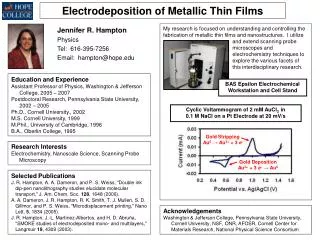
Acknowledgements • Dr. Eric Kalu • Dr. Paul Salvador • Graduate students (Andy, Bala, Nitin, Sukwon, and Pat) • CMU Materials Science Engineering Department