Supply Voltage Biasing
Supply Voltage Biasing. Andy Whetzel and Elena Weinberg University of Virginia. Agenda. Background FinFET technology Problem and approach Our design I mplementation Results Discussion Conclusion. Background. FinFET Technology Scalable Higher drive strength per unit silicon.

Supply Voltage Biasing
E N D
Presentation Transcript
Supply Voltage Biasing Andy Whetzel and Elena Weinberg University of Virginia
Agenda • Background • FinFET technology • Problem and approach • Our design • Implementation • Results • Discussion • Conclusion
Background FinFET Technology • Scalable • Higher drive strength per unit silicon Image from: http://www.ece.uc.edu/~kroenker/Research/Research%20Project%20Summaries/FINFET_image004.jpg Image from: http://www.siliconsemiconductor.net/images/news/image-76523-2012-12-12.jpg
Problem Body biasing does not work on FinFETs • MOSFET vs. FinFET: https://www.semiwiki.com/forum/content/attachments/5665d1355855218-planar-vs.-3d-finfet.jpg
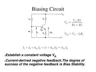
Approach Supply voltage biasing with FreePDK Contributions: • Our design for supply voltage biasing • A new knob • A new technique for decreasing delay in integrated circuits (ICs)implementing FinFET technology
Ring Oscillator • 11 Inverters • Swept bias voltage from -0.1 V to 0.1 V • 1.1 V nominal • Measured frequency, active power, and static power vs. bias voltage
NAND and NOR Gates • Designed similarly to supply biased inverter • Double the transistors, one high and one low output • Setup in ring oscillator configuration such that high output is tied to NMOS and low output is tied to PMOS in subsequent gate • Results were similar, therefore we obtained the motivation to pursue combinational logic other than a ring oscillator
Discussion • Our design shows potential to reduce delay in ICs Trade-offs: • Area • Power
Conclusion • We successfully designed and implemented a new knob • Our design decreases delay in ICs implementing FinFETtechnology • Area and power trade-offs Future Work • Further investigation of static and switching power in FinFETs under supply bias • Explore accuracy of gate induced drain leakage (GIDL) • Generating bias voltages
Image from: http://www.synopsys.com/Company/Publications/SynopsysInsight/Pages/Art2-finfet-challenges-ip-IssQ3-12.aspx


