Download
1 / 22
260 likes | 841 Vues
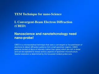
TEM Technique for nano-Science I. Convergent-Beam Electron Diffraction (CBED) Nanoscience and nanotehcnology need nano-probe!

E N D
TEM Technique for nano-Science I. Convergent-Beam Electron Diffraction (CBED) Nanoscience and nanotehcnology need nano-probe! CBED is a microanalytical technique that uses a convergent or focused beam of electrons to obtain diffraction patterns from small specimen regions. CBED patterns consist of discs of intensity (rather than spots) which are rich in detail and can be exploited to reveal various aspects of specimen microstructure. Spatial resolution is determined by the focussed incident probe size.
Convergent Beam Electron Diffraction (CBED) • Advantages: • Small probe • Rocking curve information:
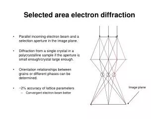
Comparing to Selected Area Electron Diffraction (SAED): SAED use parallel illumination and limits the sample volume by an aperture in the image plane of the low objective lens. A SAED pattern of a crystal. Selection area is ~0.5µm in diameter (in practice governed by aperture size) for selected area electron diffraction. We cannot get diffraction from smaller area using SAED.
Thus, CBED has higher spatial resolution than SAED. It is determined by the minimum probe diameter. More information contained in CBED pattern than spot pattern obtained with parallel electron beams: 1). specimen thickness; 2). more precise information on lattice parameters; 3). crystal system and true 3D symmetry of the atom arrangement. The price to pay is (experimental problems of CBED): 1) Contamination (CBED requires clean specimens, UHV in the microscope); 2). local specimen heating,thermal expansion, thermal stresses; If possible, use double-tilt cooling holder for the specimen.
Electron Probe: parallel or convergent? A(u)=A1(u)+A2(u), where A1(u) is a sharp peak sitting on a broad background A2(u). f: defocus value. Cs: Spherical aberration coefficient. e e sample Parallel incident beam Focused convergent beam A simulated probe using Cs=1 mm and f=-360 nm. (Zuo 2003).
How to obtain CBED patterns? • 1. Focus image at eucentric height. • 2. Excite Condenser lens C1 to yield a small spot size. • 3. Focus probe with Condenser lens C2 on to the area of interest. • 4. Press Diffraction button. • 5. Optimize pattern. Spot pattern CBED pattern: disk
CBED patterns with different convergent angle: Condenser lens aperture Condenser lens aperture e e e Small angle medium angle Large angle CBED
CBED patterns with different camera length: Large Medium Small
CBED patterns with different focus (objective lens): overfocus focus underfocus
Viewing the shadow image in CBED mode • 1. Condenser lens C2 heavily under-focussed. • 2. C2 approaching focus. • 3. C2 at focus (CBED Pattern). • 4. C2 over-focussed.
How are Kikuchi lines formed? (1) Electrons which have been inelastically scattered can subsequently be diffracted. They are observable only if they are traveling at the Bragg angle to a set of planes. (2) Two sets of electrons will be able to do this - those at +B and those at -B. (3) This diffraction results in intensity changes in the background. Because there are more electrons at B than A (since electrons passing through B are closer to the incident direction than those through A) one bright line is developed (the excess line) together with one dark line (the deficit line).
(4) Because the electrons are inelastically scattered in all directions, the diffracted electrons will form a cone, not a beam. Hence we observe Kikuchi lines - not Kikuchi spots! (5) The spacing of the pair of Kikuchi lines is the same as the spacing of the diffracted spots from the same plane. The position of the lines is very sensitively controlled by the orientation of the specimen and Kikuchi lines are often used to set the orientation of a crystal in the TEM to an accuracy of 0.01 degrees.
What is Reciprocal Lattice? Crystal structure in real space Diffraction in reciprocal space Crystalline Lattice Reciprocal Lattice
High Order Laue Zones In reciprocal lattice, all reflections (hkl) in one plane (with the normal of {uvw}) obeys zone law: h u + k v + l w = N. N is always an integer, which is called as the Laue order. [uvw] is the direction of the incident electron beam. What is HOLZ lines? Kikuchi lines also arise from inelastic scattering of HOLZ planes. They are called HOLZ lines.
Determination of crystal periodicity in the beam direction: The tenfold patterns show a tenfold distribution of the zero-order Laue zone bands and higher-order Laue zone rings indicating a periodicity of (a) 1.24 nm and (b) 3.72 nm respectively, of the Al-Cr-Cu Quasicrystals. For FOLZ ring: L: Camera Length Illustration: formation of high order Laue zone ring.
200kV Convergent Beam Electron Diffraction (CBED) High Voltage Calibration using HOLZ lines 201kV Si [331] 200kV, -180 °C, Energy-filtered (13,-13,3) (-13,13,3)
HOLZ line can be used to measure accurately the lattice parameters (A) HOLZ-line patterns obtain from several different Cu-Al alloys in the [114] direction. The HOLZ-line shifts are due to changes in lattice parameters. (B) Computer simulation of the the HOLZ pattern showing the lattice parameter that corresponds to each experimental pattern. Williams and Carter (1996).
Convergent Beam Electron Diffraction (CBED) for symmetry determination m
Phase Intergrowth Small probe can be used to identify structure from small area! Intergrowth of two orthorhombic Ga-Mn phases in form of five fold twins.
Jiang, Zuo and Spence, Acta Cryst. A 59, 341-350, (2003). Measure Low-order Structure factors Ti Charge density deformation map of TiO2 crystal along (001) plane, it pass through the center point. O
Effects of Energy-filtering: Energy filter is quite important for CBED quantitative analysis (to reduce strong background due to the large amount of thermal diffuse scattering). Unfiltered filtered, 10 ev Slit