XII. Electron diffraction in TEM
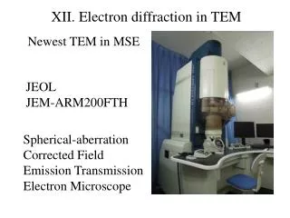
XII. Electron diffraction in TEM. Newest TEM in MSE. JEOL JEM-ARM200FTH . Spherical-aberration Corrected Field Emission Transmission Electron Microscope. Other TEM in MSE. JEOL JEM-3000F . JEOL JEM-2100 . Simple sketch of the beam path of the electrons in a TEM.

XII. Electron diffraction in TEM
E N D
Presentation Transcript
XII. Electron diffraction in TEM Newest TEM in MSE JEOL JEM-ARM200FTH Spherical-aberration Corrected Field Emission Transmission Electron Microscope
Other TEM in MSE JEOL JEM-3000F JEOL JEM-2100
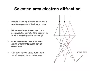
Simple sketch of the beam path of the electrons in a TEM Diffraction pattern: scattered in the same direction; containing information on the angular scattering distribution of the electrons Image plane (bottom) The diffraction pattern and the image are related through a Fourier transform.
12-1. Electron radiation (i) ~ hundreds Kev highly monochromatic than X-ray Typical TEM voltage: 100 – 400 KV Relativistic effect should be taken into account! SEM typically operated at a potential of 10 KV v ~ 20% c (speed of light) TEM operated at 200 kV v ~ 70% c.
h = 6.62606957×10⁻³⁴ m2kg/s m0 = 9.1093829110-31Kg c = 299792458 m/s e = 1.60217657×10⁻¹⁹ coulombs 1eV = 1.60217656510-19 J (Kgm2/s2)
For X-ray Wavelength = 1.542 Å J
(ii) electrons can be focused c.f. x-ray is hard to focus (iii) easily scattered : form factor for electron and x-ray, respectively Form factor for electron includes nucleus scattering! (iv) need thin crystals <1000Å, beam size m
12-2. Bragg angle is small for 100 KeV Assume d = 2Å for 200Kev
12-3. d spacing determination is not good (brevity) For fixed we can get more accurate d at higher angle! In TEM Not good for d determination!
12-4. Electron diffraction pattern from a single crystalline material Example: epitaxial PtSi/p-Si(100) Ewald sphere construction: is very smallk is very large compared to the lattice spacing in the reciprocal space
(1) An electron beam is usually incident along the zone axis of the electron diffraction pattern.
The sample can be tuned along another zone axis [xyz] . All the spots in the diffraction pattern belongs the zone axis [xyz].
12-5. Electron diffraction pattern from a polycrystalline material Example: polycrystalline PtSi/p-Si(100)
Ewald sphere constructions for powders and polycrystalline materials
12-6. diffraction and image (bright field, dark field) (a) Bright field image http://labs.mete.metu.edu.tr/tem/TEMtext/TEMtext.html
(b) Dark filed image http://labs.mete.metu.edu.tr/tem/TEMtext/TEMtext.html
Example: microcrystalline ZrO2 http://www.microscopy.ethz.ch/BFDF-TEM.htm Diffraction pattern Bright-Field Image Dark-Field Image BF image: some crystals appear with dark contrast since they are oriented (almost) parallel to a zone axis (Bragg contrast). DF image: some of the microcrystals appear with bright contrast, namely such whose diffracted beams partly pass the objective aperture.