Electron Diffraction in Crystallography: Applications and Analysis Methods
Learn about electron diffraction and its applications in crystallography, including determining crystal orientation, lattice parameters, and phases. Explore indexing diffraction patterns and practical examples.

Electron Diffraction in Crystallography: Applications and Analysis Methods
E N D
Presentation Transcript
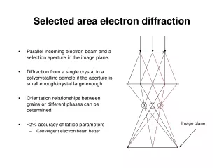
Parallel incoming electron beam and a selection aperture in the image plane. Diffraction from a single crystal in a polycrystalline sample if the aperture is small enough/crystal large enough. Orientation relationships between grains or different phases can be determined. ~2% accuracy of lattice parameters Convergent electron beam better Image plane Selected area electron diffraction
Poly crystalline sample Four epitaxial phases Diffraction with large SAD aperture, ring and spot patterns Similar to XRD from polycrystalline samples. The orientation relationship between the phases can be determined with ED.
2θ k’ k First order Laue zone Zero order Laue zone g Higher order reflections, Laue zones 2d sinθ = nλ λ200kV = 0.00251 nm Θ~1o I(k’-k)I=(2/λ)sinθB=g The intensity distribution around each reciprocal lattice point is spread out in the form of spikes directed normal to the specimen Ewald sphere (Reflecting sphere) From one set of planes we only get one reflected beam -The Bragg angle increases with increasing order (n) -Tilt sample or beam to satisfy Bragg condition of higher order reflections. k=1/λ (see figure 2.35 text book)
Double electron diffraction leads to oscillations in the diffracted intensity with increasing thickness of the sample No double diffraction with XRD, kinematical intensities Forbidden reflection may be observed t0: Extinction thickness Periodicity of the oscillations t0=πVc/λIF(hkl)I Incident beam Wedge shaped TEM sample t0 Double diffraction, extinction thickness Doubly diffracted beam Transmitted beam Diffracted beam
θB θB 2θB Objective lens Diffraction plane Excess line Deficient line 1/d Kikuchi lines Excess Deficient • Used for determination of: • crystal orientation • -lattice parameter • -accelerating voltage • -Burgers vector http://www.doitpoms.ac.uk/index.html http://www.doitpoms.ac.uk/tlplib/diffraction-patterns/kikuchi.php
Film plate Camera constant R=L tan2θB ~ 2LsinθB 2dsinθB =λ ↓ R=Lλ/d Camera constant: K=λL
(h2k2l2) Indexing diffraction patterns The g vector to a reflection is normal to the corresponding (h k l) plane and IgI=1/dnh nk nl • Measure Ri and the angles between • the reflections • - Calculate di , i=1,2,3 (=K/Ri) • Compare with tabulated/theoretical • calculated d-values of possible phases • Compare Ri/Rj with tabulated values for • cubic structure. • g1,hkl+ g2,hkl=g3,hkl (vector sum must be ok) • Perpendicular vectors: gi● gj = 0 • Zone axis:gi x gj=[HKL]z • All indexed g must satisfy: g ● [HKL]z=0 Orientations of corresponding planes in the real space
BiFeO3 Pt TiO2 Lim SiO2 Si 200 nm Example: Study of unknown phase in a BiFeO3 thin film Metal organic compound on Pt Heat treatment at 350oC (10 min) to remove organic parts. Process repeated three times before final heat treatment at 500-700 oC (20 min) . (intermetallic phase grown) Goal: BiFeO3 with space grupe: R3C and celle dimentions: a= 5.588 Å c=13.867 Å
27o 50 nm 15o 10o 0o Determination of the Bravais-lattice of an unknown crystalline phase Tilting series around common axis
0o 50 nm 19o 25o 40o 52o Determination of the Bravais-lattice of an unknown crystalline phase Tilting series around a dens row of reflections in the reciprocal space Positions of the reflections in the reciprocal space
011 111 001 101 6.04 Å 8.66 Å [101] [011] 7.94 Å 010 110 100 c b a Bravais-lattice and cell parameters [100] d = L λ / R From the tilt series we find that the unknown phase has a primitive orthorhombic Bravias-lattice with cell parameters: a= 6,04 Å, b= 7.94 Å og c=8.66 Å α= β= γ= 90o
O - K Fe - L2,3 BiFeO3 Ukjent fase 500 eV forskyvning, 1 eV pr. kanal Chemical analysis by use of EDS and EELS Ukjent fase BiFeO3 BiFe2O5
Published structure A.G. Tutov og V.N. Markin The x-ray structural analysis of the antiferromagnetic Bi2Fe4O9 and the isotypical combinations Bi2Ga4O9 and Bi2Al4O9 Izvestiya Akademii Nauk SSSR, Neorganicheskie Materialy (1970), 6, 2014-2017. Romgruppe: Pbam nr. 55, celleparametre: 7,94 Å, 8,44 Å, 6.01Å x y z Bi 4g 0,176 0,175 0 Fe 4h 0,349 0,333 0,5 Fe 4f 0 0,5 0,244 O 4g 0,14 0,435 0 O 8i 0,385 0,207 0,242 O 4h 0,133 0,427 0,5 O 2b 0 0 0,5 Celle parameters found with electron diffraction (a= 6,04 Å, b= 7.94 Å and c=8.66 Å) fits reasonably well with the previously published data for the Bi2Fe4O9 phase. The disagreement in the c-axis may be due to the fact that we have been studying a thin film grown on a crystalline substrate and is not a bulk sample. The conditions for reflections from the space group Pbam is in agreement with observations done with electron diffraction. Conclusion: The unknown phase has been identified as Bi2Fe4O9 with space group Pbam with cell parameters a= 6,04 Å, b= 7.94 Å and c=8.66 Å.