LCD INTERFACING
LCD INTERFACING. LCD OPERATION. LCD replaces LEDs Declining prices Ability to display numbers, characters and graphics Incorporation of a refreshing controller into the LCD Relieves the CPU from refreshing task Ease of programming for characters and graphics. LCD PIN DESCRIPTIONS.


LCD INTERFACING
E N D
Presentation Transcript
LCD OPERATION LCD replaces LEDs Declining prices Ability to display numbers, characters and graphics Incorporation of a refreshing controller into the LCD Relieves the CPU from refreshing task Ease of programming for characters and graphics.
LCD PIN DESCRIPTIONS 14 pins 1 – Vss , Ground 2 - Vcc , +5V 3 – VEE, for controlling LCD contrast 4 – RS, Register Select, input pin two important registers inside LCD – Command Register and Data Register. RS pin is used for the selection of these registers RS = 0 to select command register, allows user to send command such as clear display, cursor at home etc. RS = 1 to select data register allows the user to send data to be displayed on the LCD
5 – R/W • Input pin • Allows the user to write information to LCD or read information from it. • R/W = 0 for write, =1 for read 6 – E, I/O, Enable • To latch information presented to its data pins • A high to low pulse must be applied to this pin to latch information. • Minimum duration 450ns.
7 – 14, data pins, DB0 – DB7, I/O • Used to send information to LCD or to read contents of LCD’s internal registers • To display letters and numbers we send ASCII codes for the letters A - Z, a – z, and numbers 0 -9 to these pins while Rs = 1. • Use RS = 0 to check the busy flag to see if LCD is ready to receive information. • Busy flag is D7 and can be read when R/W = 1, RS = 0 • When D7 = 1, LCD is busy and D7 = 0 LCD is ready to receive new information.
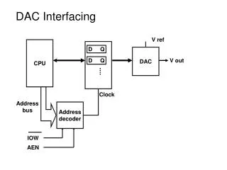
SENDING COMMANDS AND DATA TO LCD’S To send any command to LCD make pin RS = 0, for data RS = 1 Send a high to low pulse to E pin P1.0 to P1.7 are connected to LCD data pins P2.0 is connected to RS pin P2.1 is connected to R/W pin P2.2 is connected to E pin
PROGRAMME MOV A,#38H LCD 2 lines , 5x7 matrix ACALL CMTWRT ACALL DELAY MOV A, #0EH Cursor blinking ACALL CMTWRT ACALL DELAY MOV A,#01H Clear LCD ACALL CMTWRT ACALL DELAY MOV A, #’N’ display letter N ACALL DATWRT
ACALL DELAY MOV A, #’O’ Display letter O ACALL DATWRT ACALL DELAY AGAIN: SJMP AGAIN CMTWRT: MOV P1,A CLR P2.0 RS = 0 for command CLR P2.1 R/W =0 for write SETB P2.2 E = 1 for high pulse ACALL DELAY CLR P2.2 E =0 RET
DATAWRT: MOV P1,A SETB P2.0 RS=1 FOR DATA CLR P2.1 R/W = 0 SETB P2.2 E = 1 ACALL DELAY CLR P2.2 RET DELAY: MOV R4,#255 HERE: DJNZ R4, HERE RET END
ADC 0804 • WR (Set Conversion) Active low input Inform ADC to start conversion process If CS = 0 when WR makes low to high transition ADC starts converting analog signal to digital value. Time for conversion depends on CLK IN and CLK R values When conversion is completed, INTR pin becomes low.
CLK IN and CLK R • CLK IN – input pin, connected to external clock source when an external clock is used for timing. • To use the internal clock generator , the CLK IN and CLK R pins are connected to a capacitor and a resistor • In this case the clock frequency is f = 1/1.1 RC • INTR (end of conversion) • output pin, active low, normally high and at the end of conversion it goes low to signal the CPU that the data is ready to be picked up • INTR goes low , make CS = 0 and send high to low pulse to the RD pin to get the data.
Vin (+) and Vin (-) • Differential analog inputs Vin = Vin(+) – Vin(-). • Vin(-) pin is connected to ground. • Vin(+) pin is used as analog input to be converted • Vcc - +5V • Vref/2 – reference voltage, if this pin is open analog input is in the range 0 – 5V • This pin is used to implement analog voltage other than 0 – 5 v • D0 – D7 – digital data output pins, parallel ADC, tri state buffer
Analog ground and digital ground – input pins, provides ground for both analog and digital signal • Isolates analog Vin from transient voltages caused by digital switching of the output D0 – D7. • It contributes accuracy
Steps followed for data conversion • 1. make CS = 0 and send a low to high pulse to WR pin to start the conversion • 2. monitor INTR pin , if INTR is low the conversion is finished, if INTR is high keep polling until it goes low. • 3. After INTR becomes low , make CS = 0, send high to low pulse to RD pin, get data out of ADC
Programming ADC 0804 • RD – P2.5 , WR – P2.6, INTR P2.7,P1.0 – P1.7 – D0 – D7 MOV P1,#0FFH P1- INPUT PORT SETB P2.7 INTR = 1 REPRAT: CLR P2.6 WR = 0 SETB P2.6 WR – low to high transition , start conversion HERE: JB P2.7 HERE CLR P2.5 RD = 0 MOV A, P1 read data ACALL CONVERSION ACALL DISPLAY SETB P2.5 SJMP REPEAT