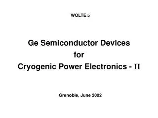
Ge Semiconductor Devices for Cryogenic Power Electronics - V
560 likes | 809 Vues
Ge Semiconductor Devices for Cryogenic Power Electronics - V. WOLTE 6. ESA/ESTEC, Noordwijk, June 2004. R. R. Ward, W. J. Dawson, L. Zhu, R. K. Kirschman GPD Optoelectronics Corp., Salem, New Hampshire O. Mueller, M. J. Hennessy, E. K. Mueller MTECH Laboratories, Ballston Spa, New York

Ge Semiconductor Devices for Cryogenic Power Electronics - V
E N D
Presentation Transcript
Ge Semiconductor DevicesforCryogenic Power Electronics - V WOLTE 6 ESA/ESTEC, Noordwijk, June 2004
R. R. Ward, W. J. Dawson, L. Zhu, R. K. KirschmanGPD Optoelectronics Corp., Salem, New Hampshire O. Mueller, M. J. Hennessy, E. K. Mueller MTECH Laboratories, Ballston Spa, New York R. L. Patterson, J. E. DickmanNASA Glenn Research Center, Cleveland, Ohio A. HammoudQSS Group Inc., Cleveland, Ohio Supported by NASA Glenn Research Center
“Very Little of the Solar System (or the Universe) Is at Room Temperature.”
TEMPERATURE CONTROL HEATING/COOLING SYSTEM CONVENTIONAL ELECTRONICS (HEAT STORAGE) THERMAL INSULATION COLD ENVIRONMENT “Traditional” Spacecraft
CRYOGENIC ELECTRONICS COLD ENVIRONMENT “Cold” Spacecraft
“Cold” Spacecraft Benefits • Eliminate heating, thermal control, isolation • Reduce power, weight, size, cost, complexity • Improve overall reliability • Reduce disruption of environment • Increase mission duration & capability
Cryogenic Power Electronics • Active semiconductor devices for power circuits • For spacecraft power management & actuator control • Parameters • Power ~10 W • Temperature range 300 K to ~20 K • Device types • Diodes (P--N, 10 A, 300 V) • JFETs (lateral, vertical) • MISFETs (lateral, vertical) • BJTs (vertical implanted) • Based on Ge
Why Ge Devices? • Applications require operation to 30 – 40 K range • Ge devices of all types can operate to low cryogenic temperatures (~20 K or lower) • Diodes • Field-effect transistors (JFETs, MISFETs) • Bipolar transistors • Performance advantages • P-N junction voltages are low • Mobility is high
Ge Cryo Power DiodesP--N Bulk Design Metal P+ implant Guard ring(s) N– ( ) Metal N+ implant
G D ~1.3 mm S S G Ge Cryo Power JFET or MISFET
Source N epitaxial layer Drain Front gate P+ implant N+ implant P+ substrate Back gate contact P+ implant Ge JFET Cross-Section (n-channel)
Ge JFET at 300 K (n-channel) 2 A ΔVGS = 1 V/step 10 V
Ge JFET at 77 K (n-channel) 2 A ΔVGS = 1 V/step 10 V
Ge JFET at 4 K (n-channel) 2 A ΔVGS = 1 V/step 10 V
Ge JFET at 300 K (p-channel) 1 A ΔVGS = 1 V/step 50 V
Ge JFET at 77 K (p-channel) 1 A ΔVGS = 1 V/step 50 V
Ge JFET at 4 K (p-channel) 1 A ΔVGS = 1 V/step 50 V
Trench Source P epitaxial layer Drain P+ implant N+ substrate Back gate contact (N+ implant) Ge JFET Cross-Section (p-channel)
Ge JFET at 300 K (p-channel) 0.5 A ΔVGS = 2 V/step 20 V
Ge JFET at 77 K (p-channel) 0.5 A ΔVGS = 2 V/step 20 V
Ge JFET at 4 K (p-channel) 0.5 A ΔVGS = 2 V/step 20 V
Ge Cryo Power MISFETs(Metal-Insulator-Semiconductor Field-Effect Transistors)
Source Gate dielectric Drain Gate N+ implant P substrate Substrate contact (P+ implant) Lateral Ge MISFET Design (n-channel)
Ge MISFET at 300 K (n-channel) 1 A ΔVGS = 1 V/step 20 V
Ge MISFET at 77 K (n-channel) 1 A ΔVGS = 1 V/step 20 V
Ge MISFET at 4 K (n-channel) 1 A ΔVGS = 1 V/step 20 V
Ge MISFET Switching - 50 kHz ~30 W Load
Ge MISFET Switching - 5 MHz ~30 W Load
Ge MISFET at 300 K (p-channel) 1 A ΔVGS = 2 V/step 20 V
Ge MISFET at 77 K (p-channel) 1 A ΔVGS = 2 V/step 20 V
Ge MISFET at 4 K (p-channel) 1 A ΔVGS = 2 V/step 20 V
Source Gate dielectric Gate P+ implant N epi P– substrate Drain P+ implant Vertical Ge MISFET Design(n-channel)
Ge Vertical MISFET at 77 K (n-channel) 0.2 A ΔVGS = 2 V/step 10 V
Ge Bipolar – Double-Implant, Vertical Emitter N+ implant Base P implant N– substrate Collector N+ implant