Download
1 / 1
10 likes | 265 Vues
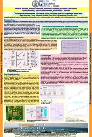
carry. carry. carry. carry. Principle of operations We have designed two types of TDC architectures in different Xilinx

E N D
carry carry carry carry Principle of operations We have designed two types of TDC architectures in different Xilinx FPGAs. Both approaches use the classic Nutt method based on the two stage interpolation.The timing acquisition process consists of three phases. First, the time interval (∆t1)between the rising edges of the START signal and the succeeding reference clock is measured. Secondly, a coarse counter is activated to measure the time interval (∆t12)between the two rising edges of the reference clock immediately following the START and the STOP signals. Finally, the same procedure for measuring the time interval (∆t2)between the rising edges of the STOP signal and the succeeding reference clock is also performed. The time interval between the START and STOP signals, ∆t, may be determined as (∆t1+ ∆t12- ∆t2). The dynamic range for fine conversion of ∆t1and ∆t2 is limited to only one reference clock cycle . COUT D 1 MUXCY c B LUT MUXCY D slice to slice delay 1 LUT c B Buffer to buffer delay max clock skew between adjacent slices is 12ps MUXCY 1 D LUT B c MUXCY 1 Start D LUT c Virtex5 slice Stop Stop Start CIN CLK (a) (b) (c) Buffer to latch delay Buffer to buffer delay Delay Cell Stop B B B B cp cp cp cp Start D Q R D Q R D Q R D Q R Reset Latch to latch delay (a) Intermediate stage TDC START STOP START Clock 100MHz D e l a y L i n e DECISION DELAY PicoBlaze MUX ∙∙∙∙∙∙∙∙∙∙∙∙ DELAY 8 ∙∙∙∙∙∙∙∙∙ 8 carry carry DELAY Converter from Termometric to Binary code 64 8 Fig.5: Communication between PicoBlaze and the TDC delay line. FF FF FF FF Alberto Aloisioa, Paolo Branchinib, Roberta Cicalesea, Raffaele Giordanoa, Vincenzo Izzoa, Salvatore Loffredob, Raffaellino Lomorob aDipartimento Scienze Fisiche, Università di Napoli “Federico II” and I.N.F.N. Sezione di Napoli - Italy b Dipartimento di Fisica, Università di Roma Tre and I.N.F.N. Sezione di Roma Tre - Italy aloisio@na.infn.it, branchini@roma3.it, cicalese@na.infn.it, rgiordano@na.infn.it, izzo@na.infn.it, loffredo@roma3.it, lomoro@roma3.it Introduction Time to Digital Converter (TDC) has been widely used in many applications such as particle detection in high energy physics, laser range finder, frequency counter and on-chip jitter measurement. For many years the main methods used to achieve the hundreds of pico-seconds resolution have been based on time-stretching, Vernier and tapped delay line. These technique were designed both in ASIC and FPGA devices. However, the design process of an ASIC device not only can be expensive, especially if produced in small quantities but also the design process is complex due to the long turn-around time and layout phase. On the other hand, low cost, fast development cycle and commercial availability are several driving motivations for using general purpose Field-Programmable Gate Arrays (FPGAs) to implement the TDC without using any external circuit. Time interval measurement literature review One of the first TDC realized on an FPGA-based approach was proposed by Kalisz, et al. [1] in 1995. They made use of the difference between a latch delay and a buffer delay of QuickLogic’s FPGA and achieved a time resolution of 100 ps. In 2003, a TDC was implemented in an ACEX 1 K FPGA from Altera by Wu, et al. [2]. This TDC used cascade chains of the FPGA and offered a time resolution of 400 ps. In the same year, Szymanowski, et al. implemented a high-resolution TDC with two stage interpolators in a QL12X16B from QuickLogic [3]. The TDC had 200 ps resolution and standard measurement uncertainty below 140 ps. In 2004, a TDC was implemented in a general purpose FPGA device by using dedicated carry lines in the FPGA to perform time interpolation by Qi An , et al [4]. Fig.1: Measurement of time interval T with the Nutt method. Our designs In the FPGA available today, there are chain structures that the vendors designed for general-purpose applications. A few well-known examples are carry chains, cascade chains, sum-of-products chains, etc. These chain structures provide short predefined routes between identical logic elements. They are ideal for TDC delay chain implementation. In our works, the fine TDC for the measurement of the short intervals, (∆t1) and (∆t2), have been performed in two different methods: 1. The first architecture, shown in Fig.2 (a) uses carry chain delays, like the one present in the newest available Xilinx Virtex 5 FPGA. The START signal after each delay unit is sampled by the pertaining flip-flop on the rising edge of the STOP signal. 2. The second architecture, shown in Fig.3 (a), uses two rows of slightly different cell delays and it makes a differential delay line by using the Xilinx Virtex 5’s slices. During the time-to-digital conversion process, the STOP pulse follows the START pulse along the line, and all latches from the first cell up to the cell where the START pulse overtakes the STOP pulse are consecutively set. To implement the designs in FPGA, one must address one major problem: in the FPGA development software, a logic cell (LE) can be physically placed in nearly any place, depending on the optimization algorithm used. When left up to the program, routing between LEs may also be unpredictable to the user. If the logic cells used for the architectures are placed and routed in this fashion, the propagation delay of each delay step will not be uniform. To avoid this, the designer is forced to place and route the logical resources by hand. The two layouts are presented respectively in Fig.2 (b) and Fig.3 (b). In Fig.2 (c) a simplified block diagrams of the Virtex 5 is shown. High-Resolution Time-to-Digital Converter in Field Programmable Gate Array High-Resolution Time-to-Digital Converter in Field Programmable Gate Array Fig.2: Carry chain delay line: (a) logic block diagram; (b) layout obtained; (c) simplified block diagram of the Virtex 5 slice. Test bench results We designed and built a PCB hosting a Virtex 5 FPGA to test the two different TDC architectures. The TDC Tester board is shown in Fig.4. Each TDC structure has 64 taps. The external clock frequency we used in the tests was 100 MHz. To execute our tests we have used an architecture based on an embedded microprocessor (Fig.5). PicoBlaze is a FPGA based microprocessor which has an 8-bit address and data port to access a wide range of peripherals.PicoBlaze allows the user to input a delayvalue via a RS232 link. The intermediate stage receives data bus, decodes it and establishes which is the value delay. Each signal is connected to the respective carry. In this way arrival time (STOP) is changed by using carry of various lengths. Carry chain has been used to generate the delays because for each step they can be considered fixed for the particular physical technology, rail voltage and temperature range. So the time interval between START and STOP has been determined and then it is measured by the TDC. Fig. 6 show a test result of the two architecture TDC outputs as a function of the signal input time. More than 1000 measurements were madeforeach point and the averageof each set of measurements was plotted. In Fig. 6 a linear fit, to guide the eye, is superimposed on experimental data. Comparable resolution, of about 80 ps have been measured for the two different delay line designs. Some non-uniformity are due to the internal layout structure of the device. Figure3: Vernier delay line: (a) logic block diagram; (b) layout obtained. (b) Fig.6: TDC output as function of the input time delay. Top: implementation of the carry delay line. Bottom: implementation of the Vernier delay line. Fig.4: TDC Tester board. [1] J. Kalisz, R. Szplet, and A. Poniecki, “Field programmable gate array based time-to-digital converter with 200-ps resolution,” IEEE Trans. Instrum. Meas., vol. 46, no. 1, pp. 51–55, Feb. 1997. [2] J. Wu, Z. Shi, and I. Y. Wang, “Firmware-only implementation of time-to-digital converter in field programmable gate array,” in Proc. IEEE Conf. Rec. NSS., vol. 1, 2003, pp. 177–181. [3] R. Szymanowski and J. Kalisz, “Field programmable gate array time counter with two-stage interpolation,” Rev. Sci. Instrum., vol. 76, 2005. 045 104. [4] Jian Song, Qi An, and Shubin Liu, “A high-resolution Time-to-Digital Converter Implemented in field programmable gate array,” IEEE Trans. Instrum. Meas., vol. 53, no. 1, Feb. 2006.