Synchronous Sequential Logic
Synchronous Sequential Logic. Chapter 5. 5- 1 Introduction. Combinational circuits contains no memory elements the outputs depends on the inputs. 5- 2 Sequential Circuits. ■ Sequential circuits a feedback path the state of the sequential circuit

Synchronous Sequential Logic
E N D
Presentation Transcript
Synchronous Sequential Logic Chapter 5
5-1 Introduction • Combinational circuits • contains no memory elements • the outputs depends on the inputs
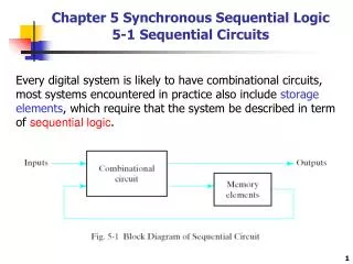
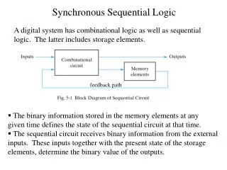
5-2 Sequential Circuits ■ Sequential circuits • a feedback path • the state of the sequential circuit • (inputs, current state) Þ (outputs, next state) • synchronous: the transition happens at discrete instants of time • asynchronous: at any instant of time
Synchronous sequential circuits • a master-clock generator to generate a periodic train of clock pulses • the clock pulses are distributed throughout the system • clocked sequential circuits • most commonly used • no instability problems • the memory elements: flip-flops • binary cells capable of storing one bit of information • two outputs: one for the normal value and one for the complement value • maintain a binary state indefinitely until directed by an input signal to switch states
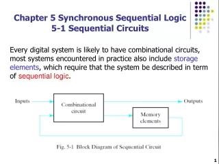
Fig. 5.2 Synchronous clocked sequential circuit
5-3 Latches • Basic flip-flop circuit • two NOR gates • more complicated types can be built upon it • directed-coupled RS flip-flop: the cross-coupled connection • an asynchronous sequential circuit • (S,R)= (0,0): no operation • (S,R)=(0,1): reset (Q=0, the clear state) • (S,R)=(1,0): set (Q=1, the set state) • (S,R)=(1,1): indeterminate state (Q=Q'=0) • consider (S,R) = (1,1) Þ (0,0)
SR latch with NAND gates Fig. 5.4 SR latch with NAND gates
SR latch with control input • C=0, no change • C=1, 1/S' S_ 0/1 R_ 1/R' Fig. 5.5 SR latch with control input
D Latch • eliminate the undesirable conditions of the indeterminate state in the RS flip-flop • D: data • gated D-latch • D Þ Q when C=1; no change when C=0 1/D' S_ 0/1 R_ 1/D Fig. 5.6 D latch
Fig. 5.7 Graphic symbols for latches
5-4 Flip-Flops • A trigger • The state of a latch or flip-flop is switched by a change of the control input • Level triggered – latches • Edge triggered – flip-flops Fig. 5.8 Clock response in latch and flip-flop
If level-triggered flip-flops are used • the feedback path may cause instability problem • Edge-triggered flip-flops • the state transition happens only at the edge • eliminate the multiple-transition problem
Edge-triggered D flip-flop • Master-slave D flip-flop • two separate flip-flops • a master flip-flop (positive-level triggered) • a slave flip-flop (negative-level triggered) Fig. 5.9 Master-slave D flip-flop
CP = 1: (S,R) Þ (Y,Y'); (Q,Q') holds • CP = 0: (Y,Y') holds; (Y,Y') Þ (Q,Q') • (S,R) could not affect (Q,Q') directly • the state changes coincide with the negative-edge transition of CP 第三版內容,參考用!
Edge-triggered flip-flops • the state changes during a clock-pulse transition • A D-type positive-edge-triggered flip-flop Fig. 5.10 D-type positive-edge-triggered flip-flop
three basic flip-flops • (S,R) = (0,1): Q = 1 • (S,R) = (1,0): Q = 0 • (S,R) = (1,1): no operation • (S,R) = (0,0): should be avoided Fig. 5.10 D-type positive-edge-triggered flip-flop
第三版內容,參考用! 1 0 1
The setup time • D input must be maintained at a constant value prior to the application of the positive CP pulse • = the propagation delay through gates 4 and 1 • data to the internal latches • The hold time • D input must not changes after the application of the positive CP pulse • = the propagation delay of gate 3 • clock to the internal latch
Summary • CP=0: (S,R) = (1,1), no state change • CP=: state change once • CP=1: state holds • eliminate the feedback problems in sequential circuits • All flip-flops must make their transition at the same time
Other Flip-Flops • The edge-triggered D flip-flops • The most economical and efficient • Positive-edge and negative-edge Fig. 5.11 Graphic symbols foredge-triggered D flip-flop
JK flip-flop • D=JQ'+K'Q • J=0, K=0: D=Q, no change • J=0, K=1: D=0 Þ Q =0 • J=1, K=0: D=1 Þ Q =1 • J=1, K=1: D=Q' Þ Q =Q' Fig. 5.12 JK flip-flop
T flip-flop • D = T⊕Q = TQ'+T'Q • T=0: D=Q, no change • T=1: D=Q' Þ Q=Q' Fig. 5.13 T flip-flop
Characteristic equations • D flip-flop • Q(t+1) = D • JK flip-flop • Q(t+1) = JQ'+K'Q • T flop-flop • Q(t+1) = T⊕Q
Direct inputs • asynchronous set and/or asynchronous reset S_ Fig. 5.14 D flip-flop with asynchronous reset reset_
5-5 Analysis of Clocked Sequential Ckts • A sequential circuit • (inputs, current state) Þ (output, next state) • a state transition table or state transition diagram Fig. 5.15 Example of sequential circuit
State equations • A(t+1) = A(t)x(t) + B(t)x(t) • B(t+1) = A'(t)x(t) • A compact form • A(t+1) = Ax + Bx • B(t+1) = Ax • The output equation • y(t) = (A(t)+B(t))x'(t) • y = (A+B)x'
State table • State transition table • = state equations
State equation A(t + 1) =Ax + Bx B(t + 1) = Ax y = Ax + Bx
State diagram • State transition diagram • a circle: a state • a directed lines connecting the circles: the transition between the states • Each directed line is labeled 'inputs/outputs‘ • a logic diagram Û a state table Û a state diagram Fig. 5.16 State diagram of the circuit of Fig. 5.15
Flip-flop input equations • The part of circuit that generates the inputs to flip-flops • Also called excitation functions • DA = Ax +Bx • DB = A'x • The output equations • to fully describe the sequential circuit • y = (A+B)x'
Analysis with D flip-flops • The input equation • DA=A⊕x⊕y • The state equation • A(t+1)=A⊕x⊕y Fig. 5.17 Sequential circuit with D flip-flop
Analysis with JK flip-flops • Determine the flip-flop input function in terms of the present state and input variables • Used the corresponding flip-flop characteristic table to determine the next state Fig. 5.18 Sequential circuit with JK flip-flop
JA = B, KA= Bx' • JB = x', KB = A'x + Ax‘ • derive the state table • Or, derive the state equations using characteristic eq.
State transition diagram State equation for A and B: Fig. 5.19 State diagram of the circuit of Fig. 5.18
Analysis with T flip-flops • The characteristic equation • Q(t+1)= T⊕Q = TQ'+T'Q Fig. 5.20 Sequential circuit with T flip-flop
The input and output functions • TA=Bx • TB= x • y = AB • The state equations • A(t+1) = (Bx)'A+(Bx)A' =AB'+Ax'+A'Bx • B(t+1) = x⊕B
Mealy and Moore models • the Mealy model: the outputs are functions of both the present state and inputs (Fig. 5-15) • the outputs may change if the inputs change during the clock pulse period • the outputs may have momentary false values unless the inputs are synchronized with the clocks • The Moore model: the outputs are functions of the present state only (Fig. 5-20) • The outputs are synchronous with the clocks
Fig. 5.21 Block diagram of Mealy and Moore state machine
5-7 Synthesizable HDL Models of Sequential Circuits • Behavioral Modeling Example: Two ways to provide free-running clock Example: Another way to describe free-running clock
Behavioral Modeling always statement Examples: Two procedural blocking assignments: Two nonblocking assignments:
Flip-Flops and Latches ■ HDL Example 5.1
Flip-Flops and Latches ■ HDL Example 5.2
Characteristic Equation Q(t + 1) = Q ⊕ T Q(t + 1) = JQ + KQ For a T flip-flop For a JK flip-flop ■ HDL Example 5.3
HDL Example 5-4 Functional description of JK flip-flop
State Diagram ■HDL Example 5.5: Mealy HDL model