VCSEL Fabrication Processing
VCSEL Fabrication Processing. The following is pictorial description of the fabrication process for oxidized VCSELs. A detailed description of each step is contained in “VCSEL Fab Details.ppt” This work was performed in Micro and Nanotechnology Laboratory at the University of Illinois

VCSEL Fabrication Processing
E N D
Presentation Transcript
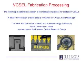
VCSEL Fabrication Processing The following is pictorial description of the fabrication process for oxidized VCSELs. A detailed description of each step is contained in “VCSEL Fab Details.ppt” This work was performed in Micro and Nanotechnology Laboratory at the University of Illinois by members of the Photonic Device Research Group
VCSEL fabrication – Bare wafer Cleave Label substrate backside Clean
VCSEL fabrication – Backside contact Target: 40 nm AuGe / 20 nm Ni / 150 nm Au
VCSEL fabrication – Spin PR Degrease /N2 dry /Dehydration bake HMDS (can spin-on or vapor prime) Spin on photoresist (usually 4330)
VCSEL fabrication – Top contact lithography 4330 lithography
VCSEL fabrication – Metal deposition O2 Plasma (300W – 3 min) 1:10 NH4OH:DI dip (15 sec) Flowing DI rinse (10 min) N2 dry, inspect, load, evaporate Target: 15 nm Ti / 150 nm Au Photonic Device Research Group
VCSEL fabrication – Liftoff Acetone soak ~5 min / Squirt gun
VCSEL fabrication – SiO2 deposition Degrease, N2 dry load, deposit dielectric > 400 nm thickness (based on color)
VCSEL fabrication – SiO2 pattern Degrease /N2 dry /Dehydration bake HMDS vapor prime Spin on AZ5214 Hardbake (110° C for 60 sec) Patern & develop
VCSEL fabrication – CF4 RIE etch Freon 14 (CF4) for > 400 nm (22 min) Remove PR mask with acetone
VCSEL – SiCl4 ICP-RIE mesa etch Clean ICP (O2 process – 15 min) ICP predep (SiCl4 recipe – 10 min) Etch > 5 mirror pair into bottom DBR To be replaced by Semigroup RIE
VCSEL fabrication – Selective oxidation Oxidation rate from test piece Use optical (below) or electrical probe Record actual pinch off in log book
VCSEL fabrication – CF4 RIE etch Freon 14 (CF4) process (~200 Å/min) Test for conduction on probe station 2 min etch, test Repeat until all SiO2 is removed
VCSEL Structure and Operation Top-view optical photograph of fabricated VCSEL Side-view schematic of fabricated VCSEL

