Soft-start
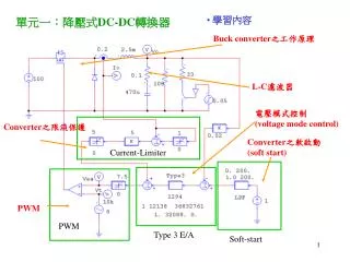
Current-Limiter. PWM. Type 3 E/A. Soft-start. 學習內容. 單元一:降壓式 DC-DC 轉換器. Buck converter 之工作原理. L-C 濾波器. 電壓模式控制 (voltage mode control). Converter 之限流保護. Converter 之軟啟動 (soft start). PWM. B2. B1. 連續導通模式 (Continuous Conduction Mode, CCM). Voltage-second 平衡 A = B.

Soft-start
E N D
Presentation Transcript
Current-Limiter PWM Type 3 E/A Soft-start • 學習內容 單元一:降壓式DC-DC轉換器 Buck converter之工作原理 L-C濾波器 電壓模式控制 (voltage mode control) Converter之限流保護 Converter之軟啟動 (soft start) PWM
B2 B1 連續導通模式 (Continuous Conduction Mode, CCM) Voltage-second 平衡 A = B
PWM (Pulse Width Modulation) • Duty ratio • Second-order low-pass filter
輸出濾波器設計 Designed with boundary condition at minimum load (Io=IoB) to ensure continuous conduction mode at any load L For High ESR C Voltage ripple due to Ro (ESR) 大小由電容材質決定 典型30~80×10-6
Design of C For Low ESR
LC-Filter Sampling Error-Amp PWM+Converter Modeling of Converter and Feedback Controller Design + Vo - + Voi - Glc VFB vcon Gpwm Gs Gea
Gain of PWM Converter And Sampling Circuits PWM+Converter Vt Vcon Vi Voi Ton Ts Sampling
Gain Characteristics of LC-Filter • Low ESR • With ESR
Type II Error Amplifier Design (For C with High ESR) • Set the crossover frequency Fco at 1/4 ~ 1/5 switching frequency (usually Fesr is lower than Fcoso the gain curve will be at –1 slope region) • Choose the error amplifier gain at Fco to be equal and opposite in dB to Gt = (Glc+Gpwm+Gs) • Fz and Fp are designed based on K-factor method to satisfy the phase margin • K = Fco/Fz= Fp/Fco
K-Factor Design 6. Assign R1 and obtain R2 K is obtained by phase margin: 7. 8. K C1 and C2
Phase lag • Phase lag of type II error Amp Fp FZ 180o from the inversion 90o from the pole at origin • Phase lag through an LC filter at Fco :
Type III Error Amplifier (For C with low ESR) • Design criterion is the same as the Type II • K-factor can be employed 1 pole
Lag Realization of Type III Error Amplifier 2 poles 1 poles Phase lag (one pole)
Experiment System Design Vi = 100.0V Vo = 50V Io(nominal) = 2A Io(min) = 0.5A Switching frequency = 10KHz Vt = 8V Minimum output ripple DV(p-p) = 100mV CCM L = 2.5mH C=125mF Low ESR High ESR C=500mF
Matlab 程式設計 % design of type 3 compensator fc=fs/5; wc=fc*2*3.1416; Hc = freqresp(H,wc); gain = 1/abs(Hc); PM=30; AngLC=-angle(Hc)*180/pi angEA=360-PM-AngLC; angK=((270-angEA)/180*3.1416)/2 K= fzero(@f3,5) fz=fc/K; fp=fc*K; R1=1.0e3 R2=gain/K*R1 C1=1/(2*pi*R2*fz) C2=1/(2*pi*R2*fp) C3=1/(2*pi*R1*fz) n=C3/C2*[1 (fz+fz)*2*pi (fz*2*pi)^2] d=[1 (C1+C2)/(R2*C1*C2) 0] G=tf(n,d); GH = series(H,G); % bode(H,G,GH); grid; clear; clc; clf; Vd=100; Vo=50; DVo=0.1; IoB=0.5; fs=10e3; Ts=1/fs; L=(Vd-Vo)*Vo*Ts/(2*Vd*IoB) C=(Vd-Vo)*Vo*Ts^2/(8*Vd*L*DVo) Ro=50e-6/C Vr=1; Vt=8.0; Gs=1/50; % Transfer functions: Gpwm+Gs+Glc pi=3.1416; num=Vd/Vt*Gs*Ro/L*[1 1/(C*Ro)]; den=[1 Ro/L 1/(L*C)]; H=tf(num,den); function y = f3(x) y = 2atan(x)-atan(1/x)-0.7517;
Gea Loop Gain Converter Converter Gea Loop Gain Fco=2kHz PM=45 K=2 系統波德圖
模擬結果 • 模擬參數設定 • PWM • 電感電流
電感電流 • 輸出電壓
Current-Limiter PWM Type 3 E/A Soft-start 實驗系統控制方塊圖
Power Module Input Power DC-DC Load 20W 60VDC AD4 AD1 PWM PCI-6025E A/D [1 4] PC 電路連接及設定
1 Simulink方塊連接