Self-assembly Nanostructure and Lithography
Self-assembly Nanostructure and Lithography. Prepared by Thu Nguyen. Self-Assembled Nanostructures.

Self-assembly Nanostructure and Lithography
E N D
Presentation Transcript
Self-assembly Nanostructure andLithography Prepared by Thu Nguyen
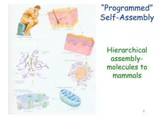
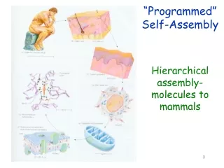
Self-Assembled Nanostructures • Self-assembled epitaxical quantum nanostructures are a class of nanostructures created by exploiting naturally occurring forces between the constituents, usually atoms and/or molecules, and a crystalline substrate such that the atoms of the resulting nanostructure have a definite spatial relationship with the underlying substrate atoms. • Since the nanostructures form during a film growth process, rather than through post-growth patterning and etching on the nanoscale, these have been dubbed self-assembled (or self-organized) nanostructures.
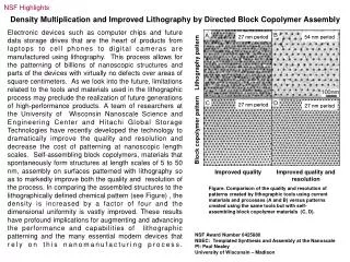
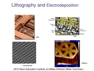
The directed self-assembly process can produce large, virtually perfect arrays of bent lines at the nanoscale. Such arrays could form the basis of nanoscale electronic devices.
Electron-beam Lithography The technique in brief consists of scanning a beam of electrons across a surface covered with a resist film sensitive to electrons, thus depositing energy in the desired pattern on the resist film. Write lines with widths of only a few nanometers in a layer of photoresist on a silicon substrate. Electron beams do not cause blurring of the edges of features because at atomic scale they don’t diffract. Can be done at nano-scale, as compared to photolithography, which is done at micro-scale. Expensive and impractical for large-scale manufacturing because the beam of electrons is needed to fabricate each structure, thus the process can be done with one line at a time.
Applications: • Application areas of e-beam lithography span a wide range from cryo-electric devices, opto-electronic devices, quantum structures, transport mechanism studies of semiconductor/superconductor interfaces, microsystem techniques, optical devices. • The use of electron-beam lithography on pentacene and poly(3-hexylthiophene) field-effect transistor to achieve device isolation and enable the realization of nanoscale organic circuits. • Can be used in the fabrication process by soft lithography.
Soft Lithography • Soft lithography uses an elastomeric mold to shape soft materials. • This technique has been recently developed as a tool for micro- and nano-fabrication (optoelectronic components)