Comprehensive Overview of Mezzanine I/O Configuration for High-Speed Data Transmission
60 likes | 163 Vues
This document provides an in-depth analysis of the mezzanine I/O configuration model, detailing the crucial components such as Serial Tx, Serial Rx, I2C communication, and the necessary data paths and control signals for efficient data handling. It covers the specifications for data readout, including bus requirements and timing constraints, while outlining the integration of FPGA, DDRAM, and various power management strategies. The focus is on enhancing data flow through serializer/deserializer configurations and their impact on system performance in real-time applications.

Comprehensive Overview of Mezzanine I/O Configuration for High-Speed Data Transmission
E N D
Presentation Transcript
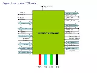
Segment mezzanine I/O model Cfg(1downto 0) Serial_Tx Data_A (15 downto 0) Serial_Rx Data_A_clk I2C_Sck Data_A _rdy I2C_Sda Data_A_ro Data_A_en-ack Jtag and config Data_B (15 downto 0) Data_B_clk Msg_data (7 downto 0) Data_B _rdy Msg_str0 Data_B_ro Msg_str1 SEGMENT MEZZANINE Data_B_en-ack B_cast_data (7 downto 0) Trig_req (1 downto 0) B_cast_str0 Trig_val (1 downto 0) B_cast_str1 Lt_data (7 downto 0) MII port Lt_Strobe LLP Status (7 downto 0) Tv_data (7 downto 0) Tv_Strobe GTS Status (7 downto 0) P3V3 P2V5 P1V5 GND
Core mezzanine I/O model Cfg(1downto 0) Serial_Tx Data_A (15 downto 0) Serial_Rx Data_A_clk I2C_Sck Data_A _rdy I2C_Sda Data_A_ro Data_A_en-ack Jtag and config Data_B (15 downto 0) Data_B_clk Msg_data (7 downto 0) Data_B _rdy Msg_str0 Data_B_ro Msg_str1 CORE MEZZANINE Data_B_en-ack B_cast_data (7 downto 0) Trig_req (1 downto 0) B_cast_str0 Trig_val (1 downto 0) B_cast_str1 Lt_data (7 downto 0) MII port Lt_Strobe LLP Status (7 downto 0) Tv_data (7 downto 0) Tv_Strobe GTS Status (7 downto 0) P3V3 P2V5 P1V5 GND
GTS mezzanine I/O model Cfg(1downto 0) Serial_Tx Serial_Rx I2C_Sck I2C_Sda Jtag and config Msg_data (7 downto 0) Msg_str0 Msg_str1 GTS MEZZANINE B_cast_data (7 downto 0) Trig_req (1 downto 0) B_cast_str0 Trig_val (1 downto 0) B_cast_str1 Lt_data (7 downto 0) MII port Lt_Strobe LLP Status (7 downto 0) Tv_data (7 downto 0) Tv_Strobe GTS Status (7 downto 0) P3V3 GND
Data readout engine 128 words/event 256 bytes/event 6 channels 1536bytes 16bit bus @ 100MHz Need 7.68µs (20µs avaible @ 50KHz) 1536*4 = 6144 byte/Event 32bit bus @ 100MHz Need 15.36µs (20µs avaible @ 50KHz) 4 pairs ; 8 I/O Serializer Data_A (15 downto 0) Deserializer Data_A_clk 32bit 32bit Data_A _rdy 512x32 DPRAM Data_A_ro To readout Engine Data_A_en-ack 9bit 9bit Serializer Data_A (15 downto 0) Data_A_clk Data_A _rdy Data_A_ro Data_A_en-ack Serializer Data_A (15 downto 0) From Trigger and readout engines Data_A_clk Data_A _rdy Data_A_ro Data_A_en-ack Data collector engine Serializer Data_A (15 downto 0) Data_A_clk Data_A _rdy Data_A_ro Data_A_en-ack
Trigger engine layout GTS CORE SEGMENT SEGMENT SEGMENT SEGMENT SEGMENT SEGMENT
ATCA carrier layout 10/100 Ethernet Switch Data Mgm FPGA Zone 3 RTM TCLK PORT GTS /SEGMENT Config µP Dual FLASH To JTAGs Data Mgm FPGA CORE /SEGMENT ZONE 2 FAST ETHERNET MAIN FPGA Data Mgm FPGA SEGMENT ZONE 2 ETHERNET 1000 PCI Express Data Mgm FPGA 32x128M SDRAM 32x512k Static DPRAM SEGMENT 8x8M FLASH POWER & IPM IMP µP DC-DC From -48v to +12/+5 DC-DC +5 +3.3 4x DC-DC +5 +3.3 DC-DC +5 +2.5 DC-DC +5 +1.2