Download
1 / 48
480 likes | 623 Vues
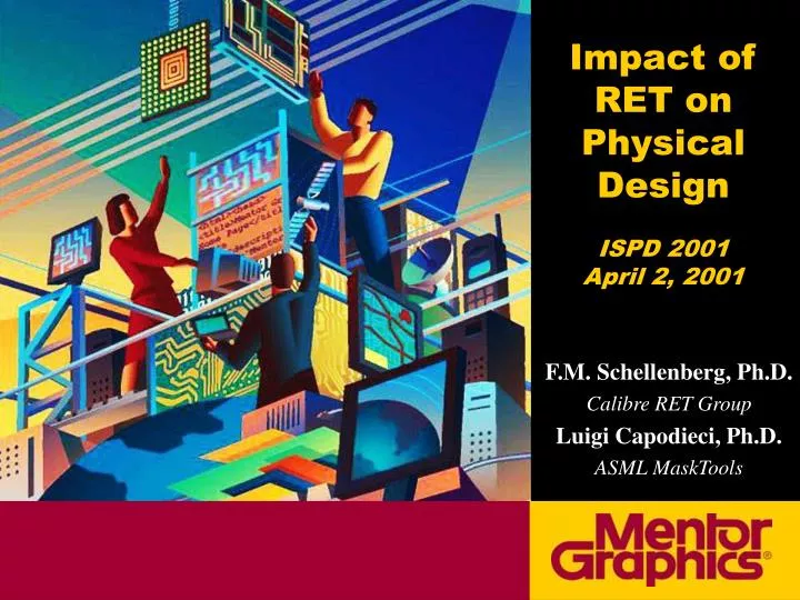
Impact of RET on Physical Design ISPD 2001 April 2, 2001. F.M. Schellenberg, Ph.D. Calibre RET Group Luigi Capodieci, Ph.D. ASML MaskTools. Agenda. Agenda Resolution Enhancement Technology (RET) Lithography Basics RET: OAI, OPC, PSM, and all that Insertion in Process Flows

E N D
Impact of RET on Physical DesignISPD 2001April 2, 2001 F.M. Schellenberg, Ph.D. Calibre RET Group Luigi Capodieci, Ph.D. ASML MaskTools
Agenda • Agenda • Resolution Enhancement Technology (RET) • Lithography Basics • RET: OAI, OPC, PSM, and all that • Insertion in Process Flows • Impact on Physical Design • OAI • OPC • PSM • Importance of a “Target” layer • Conclusions F.M. Schellenberg / ISPD 2001 / April 2, 2001
All IC layers are formed by Lithography The light interacts with a reticle (aka mask) and the lens to form a reduced image in photoresist Lithography Basics 4 UV Laser Illumination Mask Lens 100 Wafer F.M. Schellenberg / ISPD 2001 / April 2, 2001
Lithography Basics • High spatial frequencies (dense lines) scatter at larger angles. • The lens acts as a low-pass filter for high spatial frequencies F.M. Schellenberg / ISPD 2001 / April 2, 2001
Lithography Basics • Fine pitches diffract at higher angles • The lens acts recollects light onto the wafer • The lens acts like a low pass filter • “DC” light passes directly through the lens • No contrast • No image • Wasted light F.M. Schellenberg / ISPD 2001 / April 2, 2001
l Lithography Basics • The light interacting with the mask is a wave • Any wave has certain fundamental properties • Wavelength (l) • Direction • Amplitude • Phase • RET is wavefront engineering to enhance lithographyby controlling these properties Direction Amplitude Phase F.M. Schellenberg / ISPD 2001 / April 2, 2001
Wavefront Engineering: Direction l Direction Amplitude Phase F.M. Schellenberg / ISPD 2001 / April 2, 2001
Wavefront Engineering: Direction • Regular Illumination: Uniform disc • Off-Axis Illumination: e.g. Annular Lens lens Lens F.M. Schellenberg / ISPD 2001 / April 2, 2001
Wavefront Engineering: Direction • Many off-axis designs • Annular • Quadrupole / Quasar • Dipole • See your local stepper/scanner supplier or + F.M. Schellenberg / ISPD 2001 / April 2, 2001
Wavefront Engineering: Amplitude l Direction Amplitude Phase F.M. Schellenberg / ISPD 2001 / April 2, 2001
Wavefront Engineering: OPC • Optical and Process Correction (OPC)for Amplitude Control • Modifies layout to compensate for process distortions • Add light where needed • Subtract light where not wanted • Add non-electrical structures to layout to control diffraction of light F.M. Schellenberg / ISPD 2001 / April 2, 2001
Wavefront Engineering: OPC Mask layout Wafer result F.M. Schellenberg / ISPD 2001 / April 2, 2001
Wavefront Engineering: Phase l Direction Amplitude Phase F.M. Schellenberg / ISPD 2001 / April 2, 2001
Wavefront Engineering: PSM • Phase Shifting Masks (PSM) • Etch topography into mask • Creates interference fringes on the wafer • Interference fringes can be extremely small • Make mask material phase shifting • “Attenuated” PSM F.M. Schellenberg / ISPD 2001 / April 2, 2001
Wavefront Engineering: PSM Mask For conventional steppers: l=248 nm, NA=0.63 L 98 nm F.M. Schellenberg / ISPD 2001 / April 2, 2001
Wavefront Engineering: PSM • Interference effects boost contrast • Phase Masks can make extremely small gates • Phase Masks can double resolution • 2X finer pitches 90 nm SEM image courtesy of IMEC 180° 0° F.M. Schellenberg / ISPD 2001 / April 2, 2001
So What? • RET not done in isolation • Selection of RET technique carries an impact on design rules / layout restrictions F.M. Schellenberg / ISPD 2001 / April 2, 2001
Insertion points of RET • OAI: • Inserted into Lithography Stepper • OPC • Typically inserted at Physical Verification • Verification modified to include process simulation • PSM • Modify P&R rules to allow finer pitches • Insert at P&R , Physical Verification, or Mask Data Preparation F.M. Schellenberg / ISPD 2001 / April 2, 2001
Impact on Physical Design OAI OPC PSM F.M. Schellenberg / ISPD 2001 / April 2, 2001
Impact on Physical Design: OAI • Off axis amplifies certain pitches at the expense of the others. • Concept of “Forbidden” pitches Depth of Focus (a.u.) Quadrupole Illumination Half Pitch (nm) Graph reference: Noguchi, M. et al. “Subhalf Micron Lithography System with Phase Shifting Effect”, in Optical/Laser Microlithography V, Proc. SPIE Vol. 1674 (1992), 92-104. F.M. Schellenberg / ISPD 2001 / April 2, 2001
Impact on Physical Design: OAI 130 nm lines, printed at different pitchesQuasar illumination NA=0.7 Depth of Focus (mm) Acceptable Unacceptable Isolated QuasarIllumination Dense Pitch (nm) Graph reference: Socha et al. “Forbidden Pitches for 130 nm lithography and below”, in Optical Microlithography XIII, Proc. SPIE Vol. 4000 (2000), 1140-1155. F.M. Schellenberg / ISPD 2001 / April 2, 2001
Impact on Physical Design: OAI Dense Isolated 45° lines vanish 110 nm linesQuasar illumination NA=0.7 QuasarIllumination F.M. Schellenberg / ISPD 2001 / April 2, 2001
Impact on Physical Design: OAI • Quasar / Quadrupole Illumination • Amplifies dense 0°, 90 ° lines • Destroys ±45° lines • Dipole Illumination • Horizontal Dipole prints only Vertical Lines • Vertical Dipole prints only Horizontal lines • Must decompose layout for 2 exposures • Vertical mask, horizontal mask F.M. Schellenberg / ISPD 2001 / April 2, 2001
Impact on Physical Design OAI OPC PSM F.M. Schellenberg / ISPD 2001 / April 2, 2001
Impact on Physical Design: OPC • OPC changes layout dramatically • OPC does not change design F.M. Schellenberg / ISPD 2001 / April 2, 2001
Impact on Physical Design: OPC Designed Layout Mask Final Layout Wafer F.M. Schellenberg / ISPD 2001 / April 2, 2001
Impact on Physical Design: OPC Original Designed Layout Layout with OPC Graphics courtesy of IBM F.M. Schellenberg / ISPD 2001 / April 2, 2001
Impact on Physical Design: OPC SEM image courtesy of IBM F.M. Schellenberg / ISPD 2001 / April 2, 2001
Impact on Physical Design: OPC Simulation based check Graphics & SEM image courtesy of IBM F.M. Schellenberg / ISPD 2001 / April 2, 2001
Impact on Physical Design: OPC • OPC provides an automatic layout fix to achieve the target layer on the wafer • With simulation based checking, design rules can be more aggressive • Physical Verification becomes process-aware • Expands to add OPC • Verifies the results with process simulation F.M. Schellenberg / ISPD 2001 / April 2, 2001
Impact on Physical Design OAI OPC PSM F.M. Schellenberg / ISPD 2001 / April 2, 2001
Impact on Physical Design: PSM • PSM allows true resolution enhancement • Thin gates 90 nm wide in 180 nm process • Pitch doubling • Line size / pitch defined in • Libraries • Routing algorithms • Drives insertion to P&R 90 nm SEM image courtesy of IMEC F.M. Schellenberg / ISPD 2001 / April 2, 2001
Impact on Physical Design: PSM • Maskmaking concerns for PSM • Phase etch effects: linewidth imbalance • No inspection technique • No repair technique • Desire to minimize final phase area • Drives phase assignment to the last possible moment F.M. Schellenberg / ISPD 2001 / April 2, 2001
Impact on Physical Design: PSM • Best compromise: • Phase compliant Libraries, design rules • Phase assignment done at Verification • Allows PSM with OPC to be verified together • Verification includes mask manufacturing rules (e.g. imbalance). F.M. Schellenberg / ISPD 2001 / April 2, 2001
Impact on Physical Design • All RET make major changes to the layout • The “design” remains unchanged • Main consequence of RET: • Divorce between Design and Layout F.M. Schellenberg / ISPD 2001 / April 2, 2001
Impact on Physical Design “Target” Layer F.M. Schellenberg / ISPD 2001 / April 2, 2001
“Target” Layer • All RET packages have one common assumption: • The layout presented is the desired structure for the wafer • In practice, this is NOT true. F.M. Schellenberg / ISPD 2001 / April 2, 2001
“Target” Layer • Design Rules have evolved to “make things work” • These include compensations for physical phenomena (pre OPC) • The phenomena ebb and flow with process; • The rule remains as long as things work • With OPC, things may no longer work • The rules need to be reexamined F.M. Schellenberg / ISPD 2001 / April 2, 2001
“Target” Layer • Example: Historical rule on line extension • OPC software assumes the layout is the target, and adds OPC to the old OPC extension Layout according to design rule Truly desired on wafer OPC on the OPC F.M. Schellenberg / ISPD 2001 / April 2, 2001
“Target” Layer: SRAM Example F.M. Schellenberg / ISPD 2001 / April 2, 2001
“Target” Layer: Example of Embedded OPC LI Design Hand Applied OPC: A = 240nm B = 255nm C = 270nm Bit Cell Slide courtesy of LSI Logic F.M. Schellenberg / ISPD 2001 / April 2, 2001
“Target” Layer: Poly Layer De-OPC Rule Deck OPC Free Cell Slide courtesy of LSI Logic F.M. Schellenberg / ISPD 2001 / April 2, 2001
Memory Analog Mixed Signal I/O “Target” Layer Plan: De-OPC on Bit Cells OPC Free Cell Libraries Cell Libraries Compiler “Target” Layout Memory De-OPC Memory I/O I/O De-OPC Analog Analog De-OPC Mixed Signal De-OPC Mixed Signal Etc. Etc. De-OPC DRC/LVS Process-based OPC Tape Out Slide courtesy of LSI Logic F.M. Schellenberg / ISPD 2001 / April 2, 2001
“Target” Layer Conclusion • Design rules are riddled with historical OPC • DON’T DO THAT! • With systematic OPC now part of the flow,it will do the heavy lifting • Consciously clean up libraries and design rules to create the actual “target” layout • If this is not done, mysterious failures will continue F.M. Schellenberg / ISPD 2001 / April 2, 2001
Conclusions • Selection of RET is mandatory for future progress down Moore’s Law • It’s not going away • RET style has an impact on layout • Design and layout become very different • Design to a “Target” layer • Produce a layout that shows what is really desired • Allow RET to do its job F.M. Schellenberg / ISPD 2001 / April 2, 2001
Acknowledgements • Emile Sahouria, Olivier Toublan Mentor Graphics • Bob Socha, ASML • Lars Liebmann, IBM • George Bailey, LSI Logic • Kurt Ronse, IMEC F.M. Schellenberg / ISPD 2001 / April 2, 2001
Thank you for your attention. F.M. Schellenberg / ISPD 2001 / April 2, 2001
www.mentor.com F.M. Schellenberg / ISPD 2001 / April 2, 2001