Front End Processes 2006 ITRS
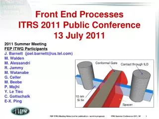
Front End Processes 2006 ITRS. 2006 FEP ITWG Team US: Raj Jammy (presenter), Jeff Butterbaugh, Mike Walden, Larry Larson Japan: Ichiro Mizushima, Masaharu Watanabe, Masaaki Niwa Europe: Mauro Alessandri, Wolfgang Mueller, Chris Stapelmann Korea: Jae-Sung Roh, Hwa-Sung Rhee, U In Chung

Front End Processes 2006 ITRS
E N D
Presentation Transcript
Front End Processes2006 ITRS 2006 FEP ITWG Team US: Raj Jammy (presenter), Jeff Butterbaugh, Mike Walden, Larry Larson Japan: Ichiro Mizushima, Masaharu Watanabe, Masaaki Niwa Europe: Mauro Alessandri, Wolfgang Mueller, Chris Stapelmann Korea: Jae-Sung Roh, Hwa-Sung Rhee, U In Chung Taiwan: Simon Jang, Vincent Chang ITRS Public Conference July 12, 2006 San Francisco
2006 FEP Sub-TWGs and Chairs • Starting Materials • Mike Walden(US), Mike Goldstein(US) • Surface Preparation • Joel Barnett(US), Karen Reinhardt(US), Chris Sparks(US) • Thermal/Thin Films/Doping • Carl Osburn(US), Hsing-Huang Tseng(US) • Etch • Greg Smith(US), Gabe Gebara(US) • Stacked DRAM • Michitaka Kubota(JP), Hideaki Fujiwara(JP) • Trench DRAM • Wolfgang Mueller(EU) • Flash • Mauro Alessandri(EU) • PCM • Mauro Alessandri(EU) • FeRAM • Jeffrey Cross(JP)
2006 FEP - Update Highlights • Starting Materials: • Minor changes • Surface Prep: • Minor changes to color coding • Red to Striped Yellow (work arounds) for Si/SiO2 loss • TTF&D: Proposed changes • Push out high-k/metal gates (2010) and FDSOI (2010) • Etch: • Added “other etch sources” section to potential solutions • Stacked DRAM: • Reviewing correlation of k w/materials • Trench DRAM: • NO will be extended down to 70nm • Non-volatile memories • Flash – STI aspect ratio requirements between NAND and NOR • PCRAM – Update requirements for phase change materials
Starting Materials2006 Update: Tables 67a and 67b • Minor changes to 2005 ITRS • Corrected colorization of particle density (Yellow to White in 2011) • Corrected colorization of particles per wafer (Yellow to White in 2011) • No other changes are applicable for the 2006 update • Focus items for the 2007 ITRS publication are being considered and a meeting will be held on August 2, 2006 in Austin to review and finalize necessary actions • Additional Emerging Materials presentations have been reviewed and discussed during 2006 – these will be taken into account for the 2007 publication
Starting MaterialsIssues / Opportunites for 2007 • Consider wafer shape interactions with immersion lithography: nanotopography and edge profile • Revisit front and back surface / edge particles • Multiple materials solutions and segmentation detracts from usefulness of generic wafer parameters applicable for today’s broad product mix • Simple SOI table may expand significantly • Emerging Materials may require separate wafer parameter list • Continue examination of 450mm: • Wafer thickness, handling, strength, edge profile/defects
Surface Preparation 2006 Updates • No Numerical Changes for 2006 Update • No typos, no misprints, no complaints • Color Change for Silicon and Silicon Oxide Loss • From RED to STRIPED YELLOW • Based on information presented at conferences • Potential Solutions • Implementation of supercritical fluids pushed out
Surface PreparationPlans for 2007 • Consider if allowable silicon/oxide loss should continue to be listed or if allowable changes in resistivity should be listed • Continue to investigate yield models for allowable particle levels with YE ITWG. Need more input from IC makers. • May need to consider “application specific” metrics for materials loss and defectivity (e.g. pre-gate, post S/D, etc.) • Incorporate results of latest survey for back surface particles (conducted at SEMATECH Surf. Prep. conference) • discussions with litho on level of “hot spot” impact • add bevel/edge metrics • Review metal contaminant classifications and consider adding other ions to metrics (e.g. SO42-). Also consider impact of SOI usage. • Discuss potential issues of immersion litho and mask cleaning with litho • Interconnect surface preparation • determine timing and requirements for ULK materials • Initiate contact cleaning metrics and ESH impact : • Increase consideration of post-CMP cleaning
Thermal, Thin Films, & Doping Updates and Issues • Date for High-k/ Metal Gate for High Performance Likely to be Moved Out from 2008 to 2010 • Need to revisit and re-examine assumptions in scaling criteria • Stress enhancement must be factored in to scaling options • PIDS dependency • Date for Expected First Shift from Bulk to FDSOI Now Expected to be 2010, Rather Than 2008 - Too Many Unknowns: Availability of 7nm ± 10% Material Channel Mobility in thin Si layers High k/Metal Gate Availability - Table Remains Unchanged Since Bulk and FDSOI Overlap - Date for Switch to FDSOI is also tied to High k/Metal Gate • 2005 Reductions in Junction Depth and Series Resistance Remain Problematic (Unrealistically Aggressive) and are a Candidate for Revision in 2007
Comparison of 2004 and 2005 ITRS Junction Parameters Requirements Have Dramatically Increased
Etch 2006 Updates • %CD variation line in (design) Table 18a changes from 10% to 12% • Revised “Etch Potential Solutions Table” for Fig. 60.
Etch Plans for 2007 • Review resist aspect ratio requirements for trimming, recommend inclusion of line in table. • Resist collapse during trim is becoming a problem. • May drive multilayer resist or hard mask • Need to examine process parameters fro litho develop and trim • Need to explicitly call out hard mask parameters in the table • Lg: scaling and CD uniformity and CD tolerance • Litho improvements allow for CDU to go down from 3.6 to 3.2 nm • Restricting the pitch will help in improving CD uniformity • Multiples of narrow pitch across the chip would help litho reduce the CDU to 1.6 nm from 3.2 nm (3s) : DFM solution • Incorporate results of survey of actual physical gate length, to be conducted starting in July.
Stacked DRAM 2006/2007 Updates and Issues • No change in Table 70 and texts. • Correction in Fig. 61 is desirable to match the timing of the change of material and dielectric constant in Table 70. • Combination of high-k dielectrics may be used to achieve desired k WAS IS
Stacked DRAM Plans for 2007 • Incorporate PIDS DRAM survey results in 2007 FEP • Consider transfer of FEP Stacked DRAM section to Korea DTWG
Trench DRAM 2006 Updates • For capacitor dielectric NO will be extended down to 70nm. High k materials such as Al2O3 or HfSiON will be used from 65nm onwards. • New integration schemes to be introduced for 40nm will reduce the temperature budget for the cell capacitor. Thus a more aggressive scaling of the capacitance equivalent oxide thickness (CET) will be possible. As a consequence the trench aspect ratio can be kept at less/equal than 100 down to 28nm.
Trench DRAM Plans for 2007 • Discuss and consolidate with Stacked DRAM the parameters in the tables where possible • Review with Stacked DRAM the roadmap beyond 30nm • Can an evolutionary roadmap be sustained beyond 30nm? • Have new cell structures to be included in the roadmap?
Flash Memory2006 Updates • Add requirements for STI isolation
Flash Memory Plans for 2007 • Discuss the end date for the roadmap of stacked gate Flash architecture and agree with PIDS • Deep review of the evolution and requirements for tunnel and interpoly dielectrics • Separation of NAND and NOR for STI requirements • Implementation of more new architectures to be discussed, i.e. nanodots, nitride floating gate, etc. • ERD considers these options to be mature for transfer to FEP
Phase Change Memory (PCM)2006 Updates • Add first requirements for phase change material Plans for 2007 • Review and expand requirements for phase change material • Add requirements for heater material • Definition of appropriate production volumes/year
FeRAM 2006 Updates • No Change in Tables • A few comments related to the 2005 text: • For clarification • Additional description about new materials
FeRAM Plans for 2007 • Ongoing Survey of Commercial FeRAM Production Status • Definition of Production Year Appropriate for FeRAM • 10kp/month volume by 2 companies (as with DRAM) ? • Common Half Pitch Standard is Desirable to be applied also to other new memories • Scaling Rate of FeRAM is Subject of Ongoing FEP/PIDS Discussion
2007 FEP – Summary of Current Plans • Starting Materials: • Wafer shape interactions with immersion Litho • Possible expansion of SOI tables • Emerging materials may require separate wafer parameter requirements • Surface Prep: • May need to consider “application specific” metrics for materials loss and defectivity (e.g. pre-gate, post S/D, etc.) • Continued examination of back surface particles metric • TTF&D: • All models/assumptions to be revisited for projections and timing • Junction depth and series R parameters unrealistically aggressive – to be revisited
2007 FEP – Summary of Current Plans • Etch: • Review resist aspect ratio requirements for resist collapse during trim • Survey of actual physical gate length – trim, tolerance & uniformity • DRAM: • Coordinate trench and stack scaling parameters • Flash: • Discussion on end of stacked gate flash roadmap and new cell architectures • Deep review of IPD and tunnel dielectric requirements/scaling options • Separation of NOR vs NAND scaling and impact on STI aspect ratio • PCRAM: • Review and expand requirements for phase change and heater materials • Discussion on production volumes/metrics and definition of half pitch stds • FERAM: • Continued discussion on production volumes/metrics and definition of half pitch stds

